IC Integration Enables Flat-Panel Phased Array Antenna Design
IC Integration Enables Flat-Panel Phased Array Antenna Design
by
Jeff Lane
Sep 1 2020
Abstract
Advances in semiconductor technology have enabled the proliferation of phased array antenna across the industry. This shift away from the mechanically steered antenna to the active electronically scanned antenna (AESA) began years ago in military applications, but has rapidly advanced more recently in satcom on-the-move and 5G communications. The low profile AESA has advantages such as fast steering capability, the ability to produce multiple radiation patterns, and higher reliability; however, these antennas required significant advancements in IC technology before they could become widely available. Planar phased arrays require devices operating with high levels of integration, low power consumption, and high efficiency so that users may fit these components behind the antenna array while keeping the heat generated to acceptable levels. This article will briefly describe how advances in phased array chipsets are making planar phased array antennas possible, followed by examples.
Introduction
In past years, parabolic dish antennas have been widely used to transmit and receive signals where directivity is important. Many of those systems work well and have a relatively low cost after years of optimization. These mechanically steered dish antennas do have some drawbacks. They are physically large, slow to steer, have worse long-term reliability, and they offer just one desired radiation pattern or data stream.
Phased array antennas are electrically steered and offer numerous benefits such as having a lower profile, less volume, improved long-term reliability, faster steering, and multiple beams. A key aspect of the phased array antenna design is the spacing of the antenna elements. The approximately half-wavelength element spacing needed for most arrays creates particularly challenging designs at higher frequencies. This drives the ICs at higher frequencies to be increasingly integrated and packaging solutions to become more advanced.
There has been strong interest in using phased array antenna technology for various applications. However, engineers have been limited by the ICs available to make them feasible. This is no longer the case due to recent developments in IC chipsets. Semiconductor technology is moving toward advanced siliconICs where we can combine digital controls, memory, and RF transistors onto the same IC. Also, gallium nitride (GaN) is significantly increasing the power density of power amplifiers to offer a much smaller footprint.
Phased Array Technology
There is a major push in the industry toward low profile arrays that consume less volume and weight. The traditional plank architecture essentially uses small PCB planks with electronics on them perpendicularly fed into the back side of the antenna PCB. This approach has been improved over the past 20 years to continually reduce the size of the plank, thereby reducing the depth of the antenna. Next-generation designs move from this plank architecture to a flat- panel approach. Flat-panel designs significantly reduce the depth of antennas, making them easier to fit into portable or airborne applications. Achieving smaller size requires enough integration in each IC to fit them on the back side of the antenna.
In planar array designs, the space available for ICs on the back side of the antenna is limited by the antenna element spacing. As an example, the maximum antenna element spacing to prevent grating lobes for up to a 60° scan angle is 0.54 λ. Figure 1 shows this maximum element spacing in inches vs. frequency. As you go higher in frequency, the spacing between the elements becomes quite small, leaving little room for components behind the antenna.

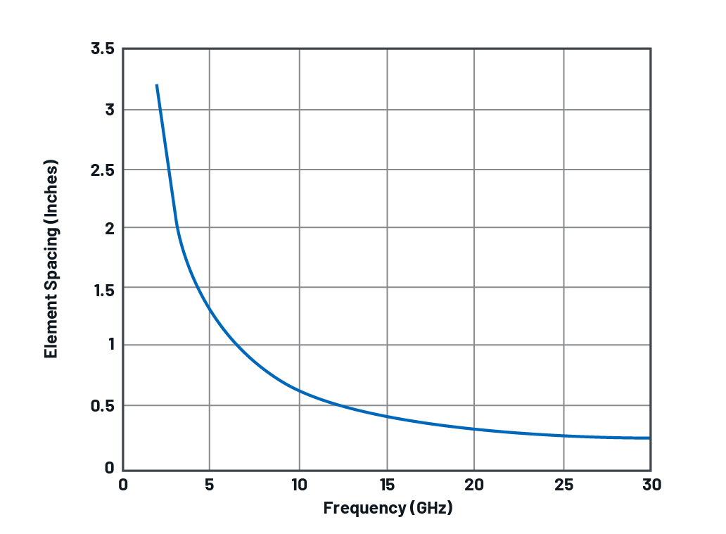
Figure 1. Antenna element spacing to prevent grating lobes at 60° off-boresight.
In Figure 2, the image on the left shows the gold patch antenna elements on the top side of the PCB and the image on the right shows the analog front end of the antenna on the bottom side of the PCB. A frequency conversion stage and distribution network on additional layers are also typical in these designs. It can easily be seen that more integrated ICs significantly reduce the challenges in laying out the antenna design with the required spacing. As the antenna becomes smaller with more electronics packed into a reduced footprint, it demands new semiconductor and packaging technology to help make the solutions viable.

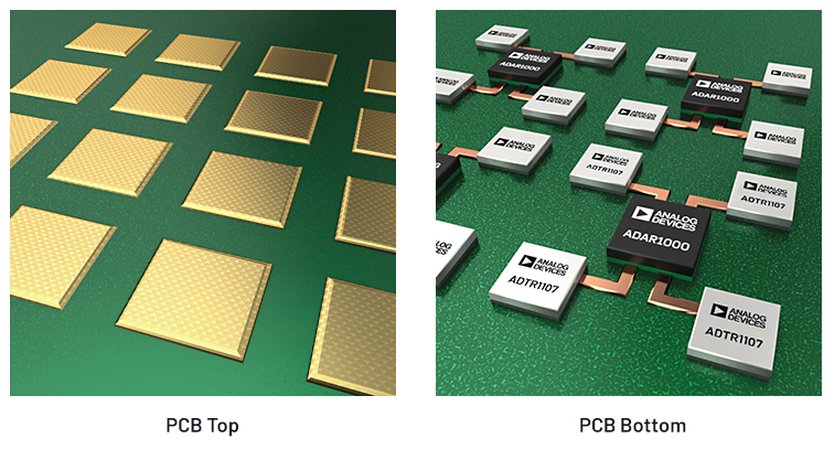
Figure 2. Flat-panel array showing antenna patches on the top side of a PCB, as well as the ICs on the back side of an antenna’s PCB.
Semiconductor Technology and Packaging
The microwave and millimeter wave (mmW) IC components used as building blocks for a phased array antenna are shown in Figure 3. In the beamforming section, the attenuator adjusts the power level at each antenna element so that the sidelobes of the antenna pattern can be reduced. The phase shifter adjusts the phase of each antenna element to steer the antenna main beam, and a switch is used to toggle between transmitter and receiver paths. In the front-end IC section, a power amplifier is used for the transmit signal, a low noise amplifier is used for the received signal, and, finally, another switch is used to toggle between the transmitter and receiver. In past implementations, each of these ICs was offered as separate packaged devices. More advanced solutions could have an integrated monolithic single-channel gallium arsenide (GaAs) IC to achieve this functionality. Not shown, but included in most arrays before the beamformer, are a passive RF combiner network, receiver/exciter, and signal processor.

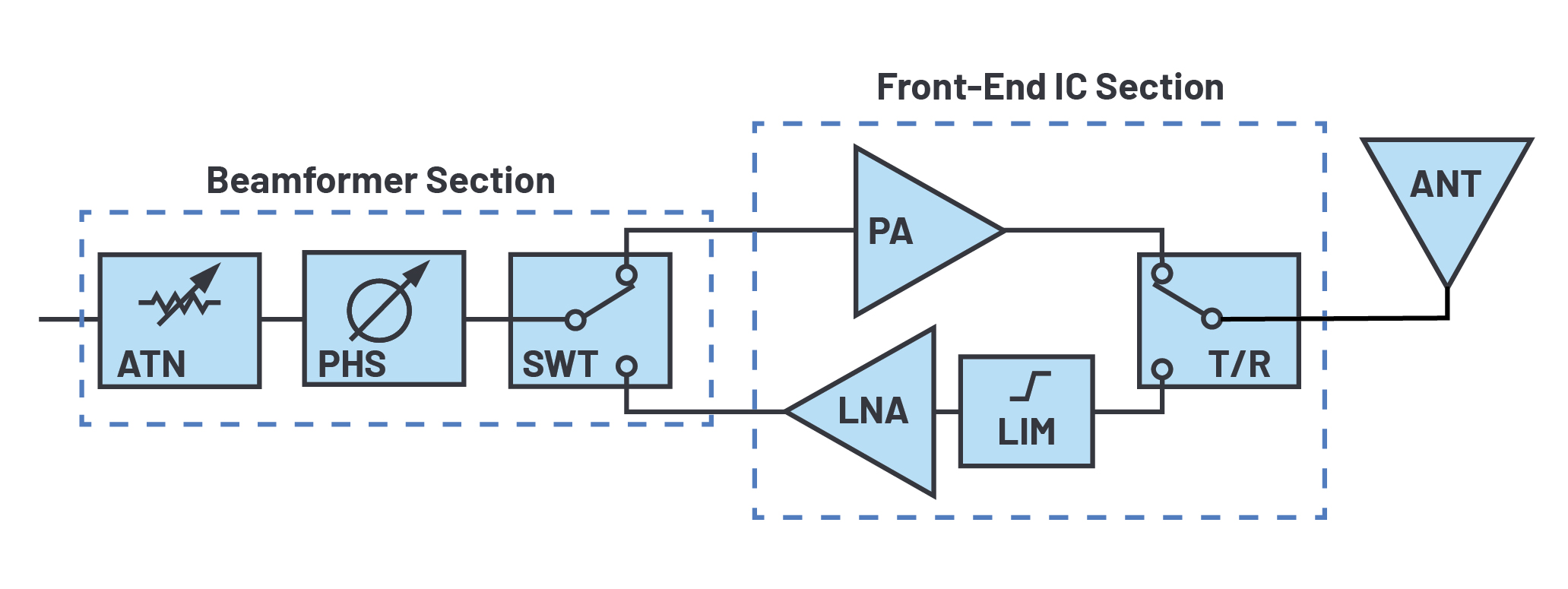
Figure 3. Typical RF front end of a phased array antenna.
The recent proliferation of phased array antenna technology has been aided by advancements in semiconductor technology. The advanced nodes in SiGe BiCMOS, silicon-on-insulator (SOI), and bulk CMOS have combined digital and RF circuitry. These ICs can perform the digital tasks in the array, as well as control the RF signal path, to achieve the desired phase and amplitude adjustment. It’s possible today to achieve multichannel beamforming ICs that perform gain and phase adjustment in a 4-channel configuration, as well as up to 32 channels aimed at mmW designs. In some lower power examples, a silicon-based IC could be a monolithic solution for all the previous functions. In high power applications, gallium nitride-based power amplifiers significantly increased the power density that may be fit into the unit cell of a phased array antenna. These amplifiers would have traditionally used traveling wave tube (TWT)-based technology or relatively low power GaAs-based ICs.
In airborne applications, we are seeing a trend to flat-panel architectures with the power added efficiency (PAE) benefits of GaN technology. GaN has also enabled large ground-based radars to move from a dish antenna, driven by a TWT, to phased array-based antenna technology, driven by solid-state GaN ICs. We are now able to have monolithic GaN ICs capable of delivering over 100 W of power with over 50% PAE. Combining this level of efficiency with the low duty cycle of radar applications allows for surface-mount solutions where we can dissipate the heat generated through the package base. These surface-mount PAs greatly reduce the size, weight, and cost of the antenna array. The additional benefit beyond the pure power capability of GaN is the size reduction compared to existing GaAs IC solutions. As an example, a 6 W to 8 W GaN-based power amplifier at X-band reduces the footprint by 50% or more vs. a GaAs-based amplifier. This footprint reduction is significant when trying to fit these electronics into the unit cell of a phased array antenna.
Advancements in packaging technology also enable planar antenna architectures at a much lower cost. High reliability designs may use gold plated, hermetically sealed housing with chip-and-wire interconnects inside. These housings may be more robust for extreme environments, but are large and costly. Multichip modules (MCMs) combine multiple MMIC devices, as well as passives, into a relatively low cost surface-mount package. MCMs still allow for the mixing of semiconductor technologies so that the performance of each device can be maximized while saving considerable space. For example, in the case of a front-end IC, it may contain a PA, an LNA, and a T/R switch. The thermal vias or the solid copper slug in the base of the package is used to get the heat out. Commercial, military, and space applications, with the desire to save on costs, are now using the significantly lower cost surface-mount packaging alternatives in many applications.
Phased Array Beamformer ICs
Integrated analog beamforming ICs, often called core chips, are aimed at supporting a range of applications including radar, satellite communications, and 5G telecommunications. The primary function of these chips is to accurately set the relative gain and phase of each channel so that signals add coherently in the desired direction of the antenna main beam. They are being developed for analog phased array applications or hybrid array architectures that combine some digital beamforming with analog beamforming.
The ADAR1000 X-/Ku-band beamforming IC is a 4-channel device covering 8 GHz to 16 GHz operating in time division duplex (TDD) mode with the transmitter and receiver integrated into one IC. In receive mode, input signals pass through four receive channels and are combined in a common RF_IO pin. In transmit mode, the RF_IO input signal is split and passes through the four transmit channels. A functional diagram is shown in Figure 4.

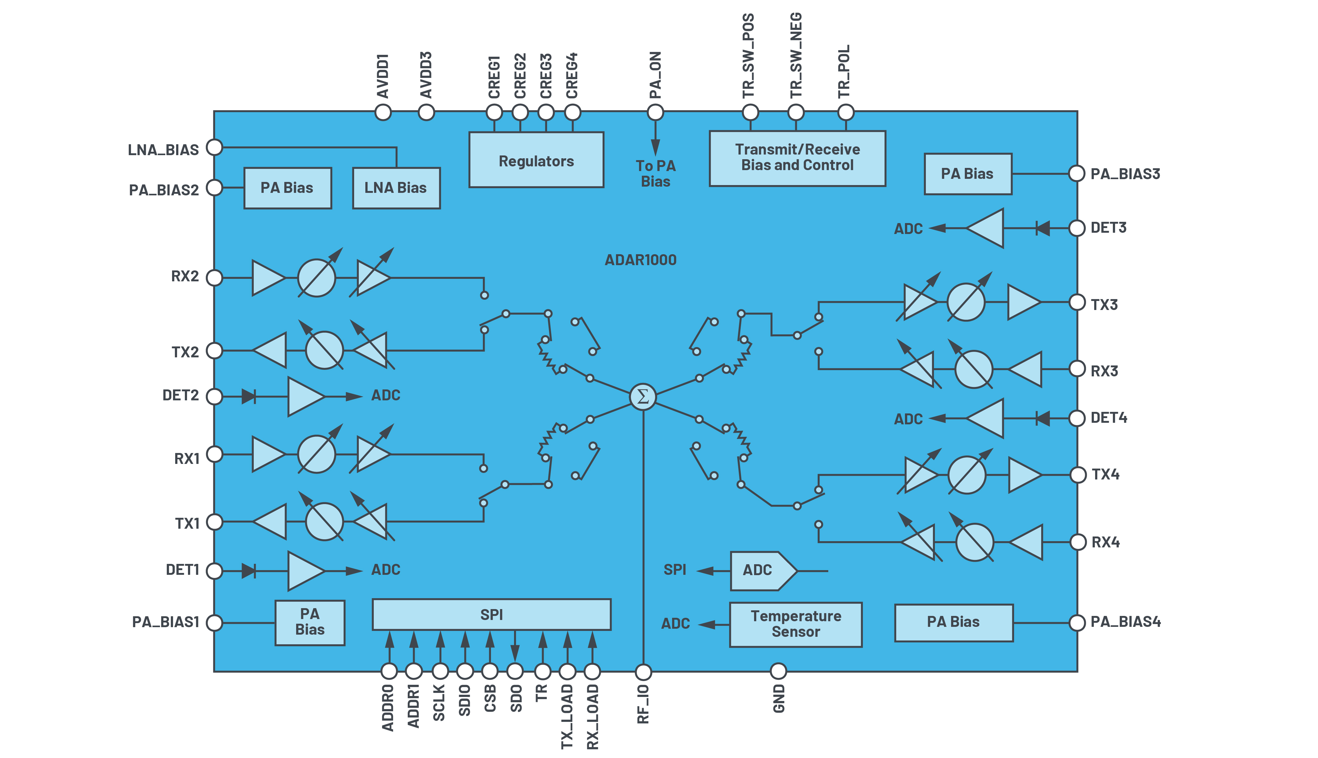
Figure 4. ADAR1000 functional block diagram.
A simple 4-wire serial port interface (SPI) controls the on-chip registers. Two address pins allow SPI control of up to four devices on the same serial lines. Dedicated transmit and receive pins provide synchronization of all core chips in the same array. A single pin controls fast switching between the transmit and receive modes. The 4-channel IC is housed in a 7 mm × 7 mm QFN surface-mount package for easy integration into flat-panel arrays. The high level of integration, coupled with a small package addresses some of the size, weight, and power challenges in high channel count phased array architectures. The device dissipates only 240 mW/channel in transmit mode and 160 mW/channel in receive mode per channel.
The transmit and receive channels are brought directly external and designed to mate with a front-end IC. Figure 5 shows plots of gain and phase for the device. A full 360° phase coverage with phase steps less than 2.8° and over 30 dB of gain adjustment is achieved. The ADAR1000 contains on-chip memory to store up to 121 beam states where one state contains all phase and gain settings for the entire IC. The transmitter delivers approximately 19 dB gain with 15 dBm of saturated power, where the receive gain is approximately 14 dB. Another key metric is the phase change over gain setting, which is approximately 3° over a 20 dB range. Similarly, the gain change with phase is about 0.25 dB over the entire 360° phase coverage, which eases the calibration challenges.

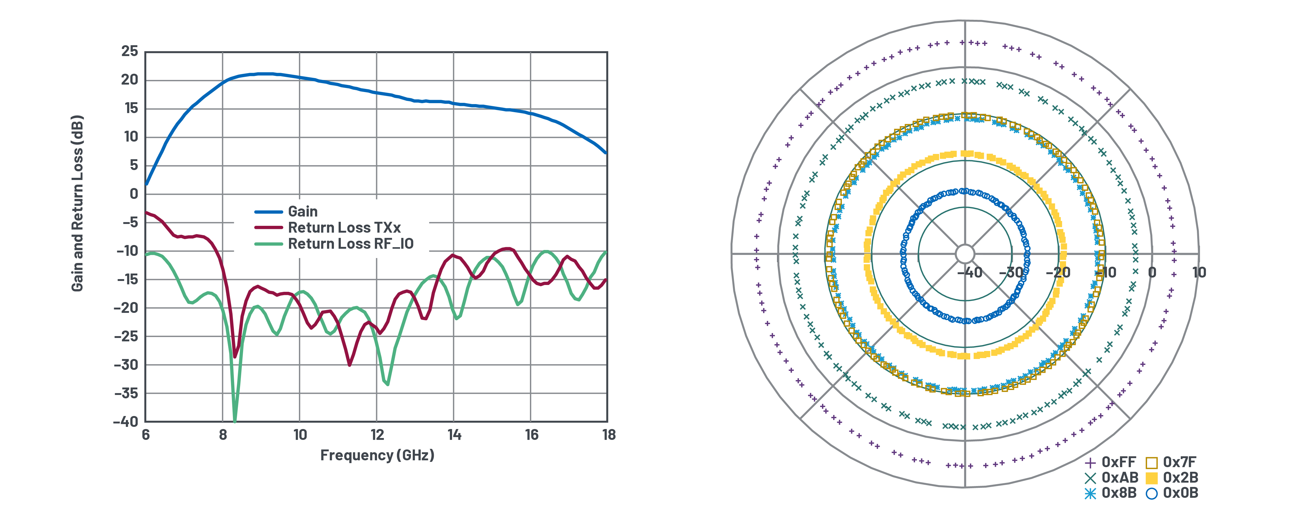
Figure 5. ADAR1000 transmit gain/return loss and phase/gain control, where frequency = 11.5 GHz.
A complement to the ADAR1000 beamforming chip is the front-end IC, ADTR1107. The ADTR1107 is a compact, 6 GHz to 18 GHz, front-end IC with an integrated power amplifier, low noise amplifier (LNA), and a reflective single-pole, double-throw (SPDT) switch. A functional block diagram is shown in Figure 6.

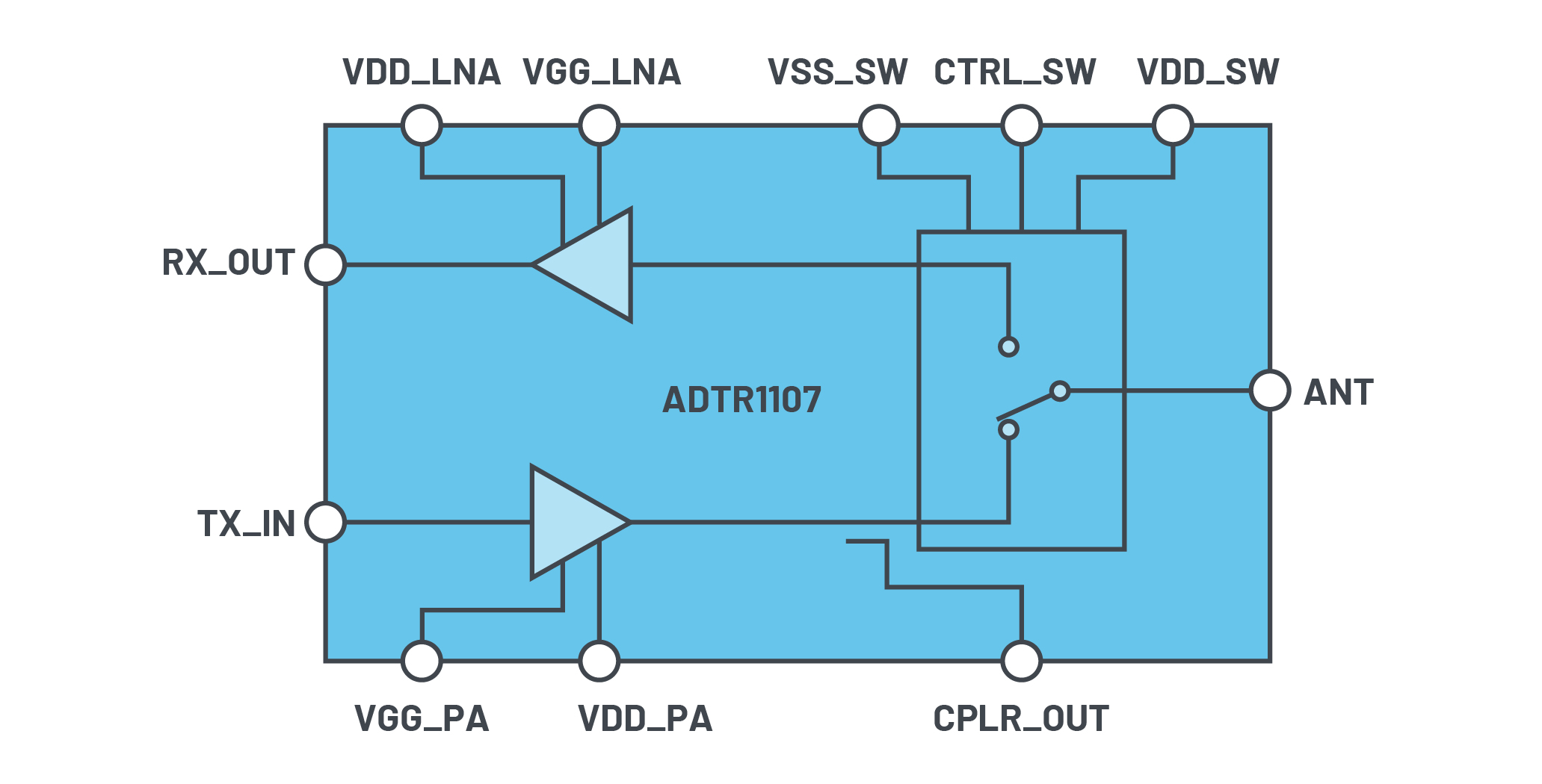
Figure 6. ADTR1107 functional block diagram.
This front-end IC offers 25 dBm of saturated output power (PSAT) and 22 dB small signal gain in the transmit state, and 18 dB small signal gain and 2.5 dB noise figure (including the T/R switch) in the receive state. The device has a directional coupler for power detection. The input/outputs (I/Os) are internally matched to 50 Ω. The ADTR1107 is supplied in a 5 mm × 5 mm, 24-lead, land grid array (LGA) package. The transmit and receive gain and return loss of the ADTR1107 are shown in Figure 7.

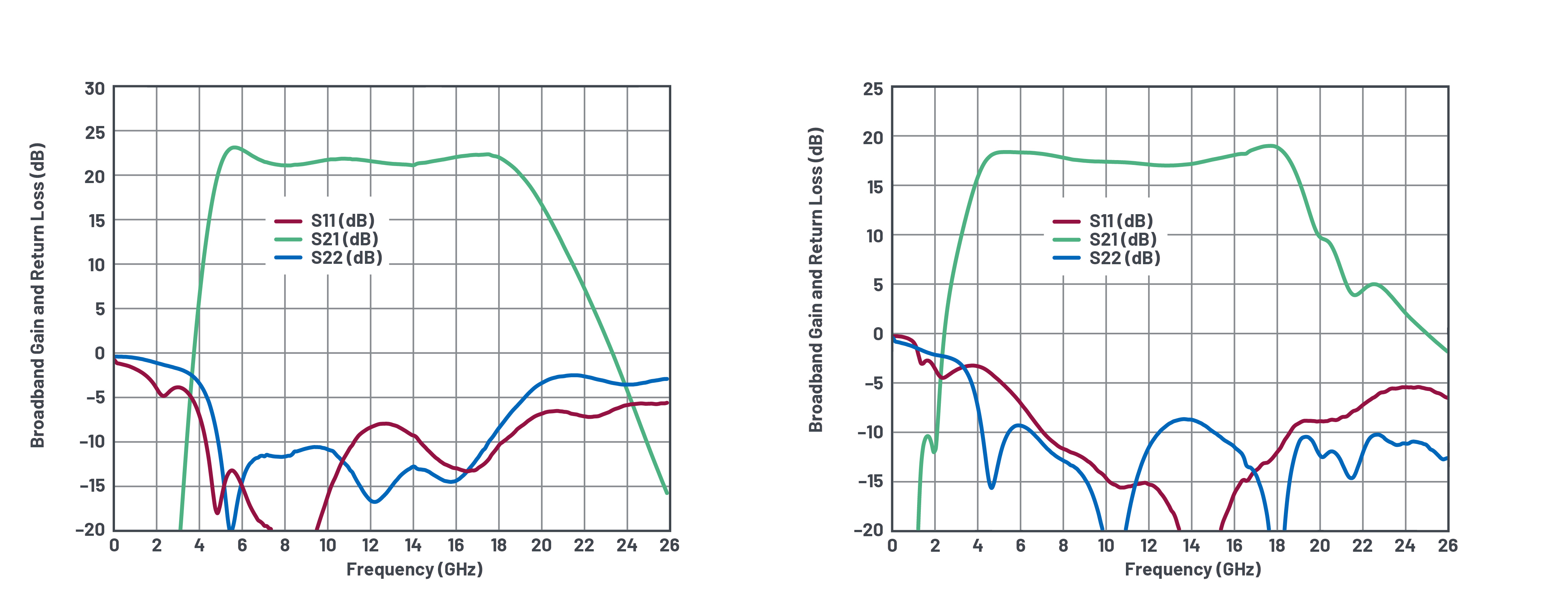
Figure 7. ADTR1107 transmit gain/return loss and receive gain/return loss.
The ADTR1107 has been designed for easy integration with the ADAR1000. An interface schematic is shown in Figure 8. Four ADTR1107 ICs are driven by a single ADAR1000 core chip. For simplicity, the connections for only one of the four ADTR1107 ICs are shown.

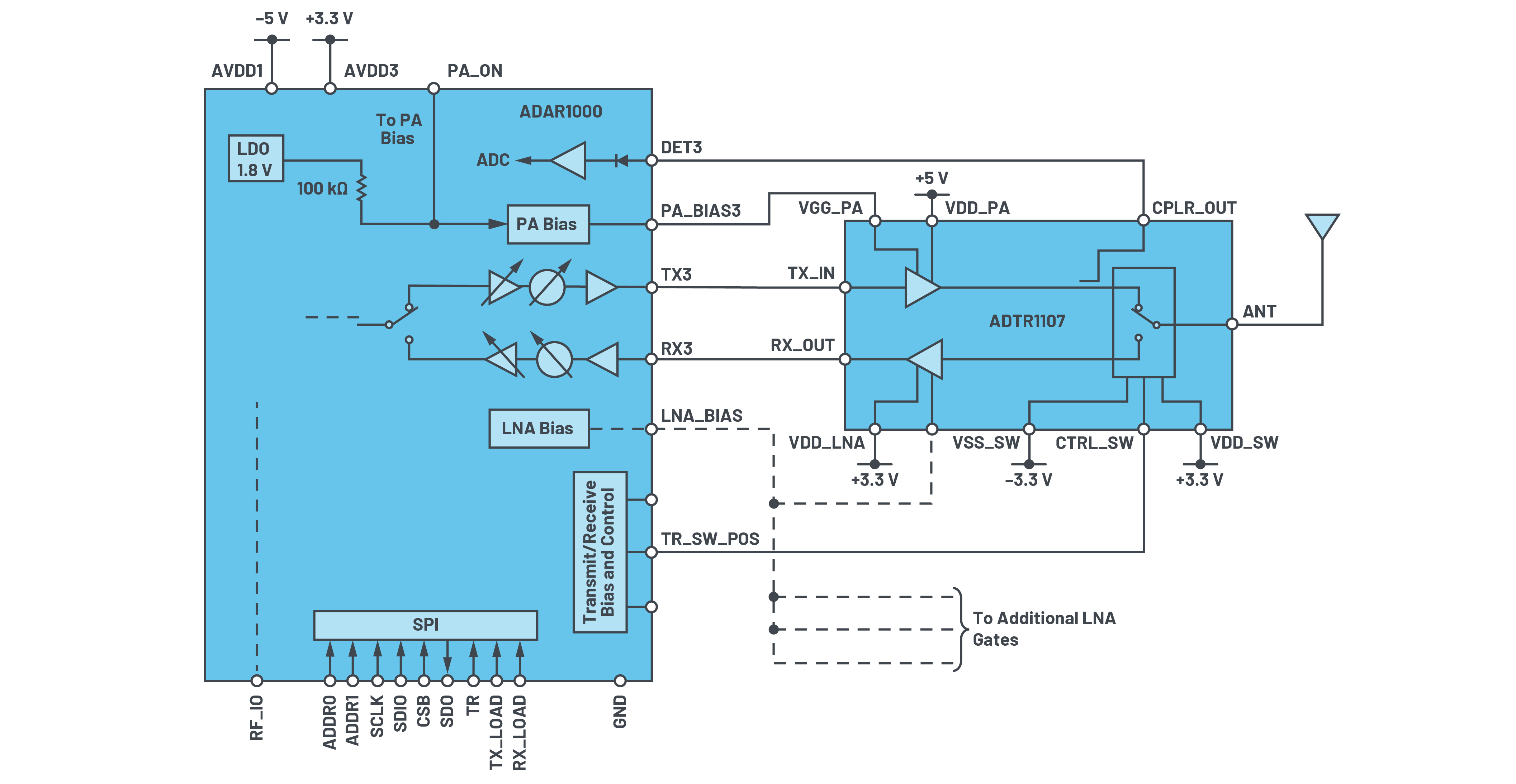
Figure 8. Interfacing the ADTR1107 frond-end IC to the ADAR1000 X-band and Ku-band beamformer.
The ADAR1000 provides all of the required gate bias voltages and control signals, resulting in a seamless interface to the front-end IC. While the ADTR1107 LNA gate voltage is self-biased, the voltage can also be controlled from the ADAR1000. The gate voltage for the ADTR1107 power amplifier is also provided by the ADAR1000. Four independent negative gate voltages are needed for power amplifier gate biasing since one ADAR1000 drives four ADTR1107s. Each voltage is set by an 8-bit digital-to-analog converter (DAC). This voltage can be asserted by the ADAR1000 TR input or by a serial peripheral interface write. Asserting the ADAR1000 TR pin switches the polarity of the ADAR1000 between receive and transmit modes. The TR_SW_POS pin can drive the gates of up to four switches and can be used to control the ADTR1107 SPDT switch.
The ADTR1107 CPLR_OUT coupler output can be tied back to one of the four ADAR1000 RF detector inputs (DET1 to DET4 in Figure 4) to measure transmit output power. These diode-based RF detectors have an input range of −20 dBm to +10 dBm. The coupling factor of the ADTR1107 directional coupler ranges from 28 dB at 6 GHz to 18 dB at 18 GHz.
Pulsing of the ADTR1107 can be achieved via the gate voltage driven by the ADAR1000 while the drain is held constant. This is superior to pulsing via the drain as this would require a high power MOSFET switch and gate driver device vs. gate switching, which is low current. It should also be noted that the ADAR1000 puts out sufficient power to saturate the ADTR1107 in transmit mode, and the ADTR1107 is designed to survive the total reflected power in the case of a shorted antenna.
The combined performance of the ADTR1107 and the ADAR1000 in both transmit and receive modes over a frequency range from 8 GHz to 16 GHz are shown in Figure 9. In transmit mode, they provide approximately 40 dB of gain and 26 dBm of saturated power, while in receive mode they provide approximately 2.9 dB of noise figure and 25 dB of gain.

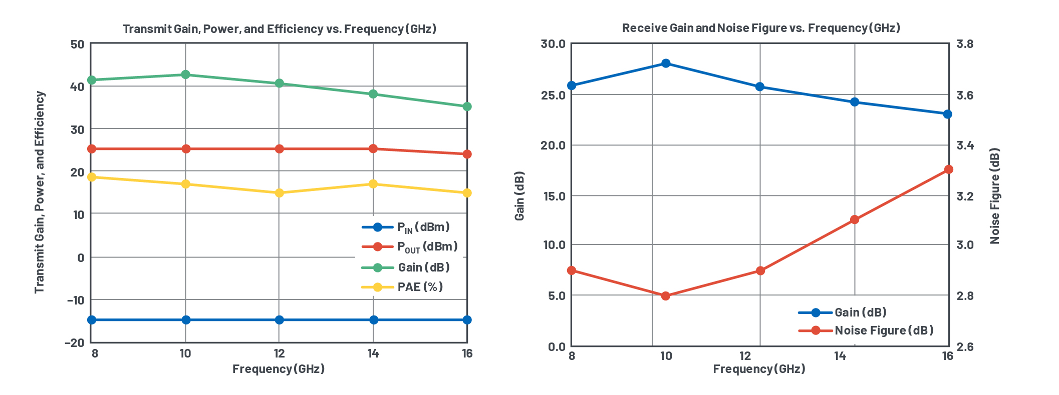
Figure 9. Transmit and receive performance of ADTR1107 coupled with ADAR1000 (single channel).
Figure 10 shows four ADAR1000 chips driving 16 ADTR1107 chips. A simple 4-wire SPI controls all of the on-chip registers. Two address pins allow SPI control of up to four ADAR1000 chips on the same serial lines. Dedicated transmit and receive load pins also provide synchronization of all core chips in the same array, and a single pin controls fast switching between the transmit and receive modes.

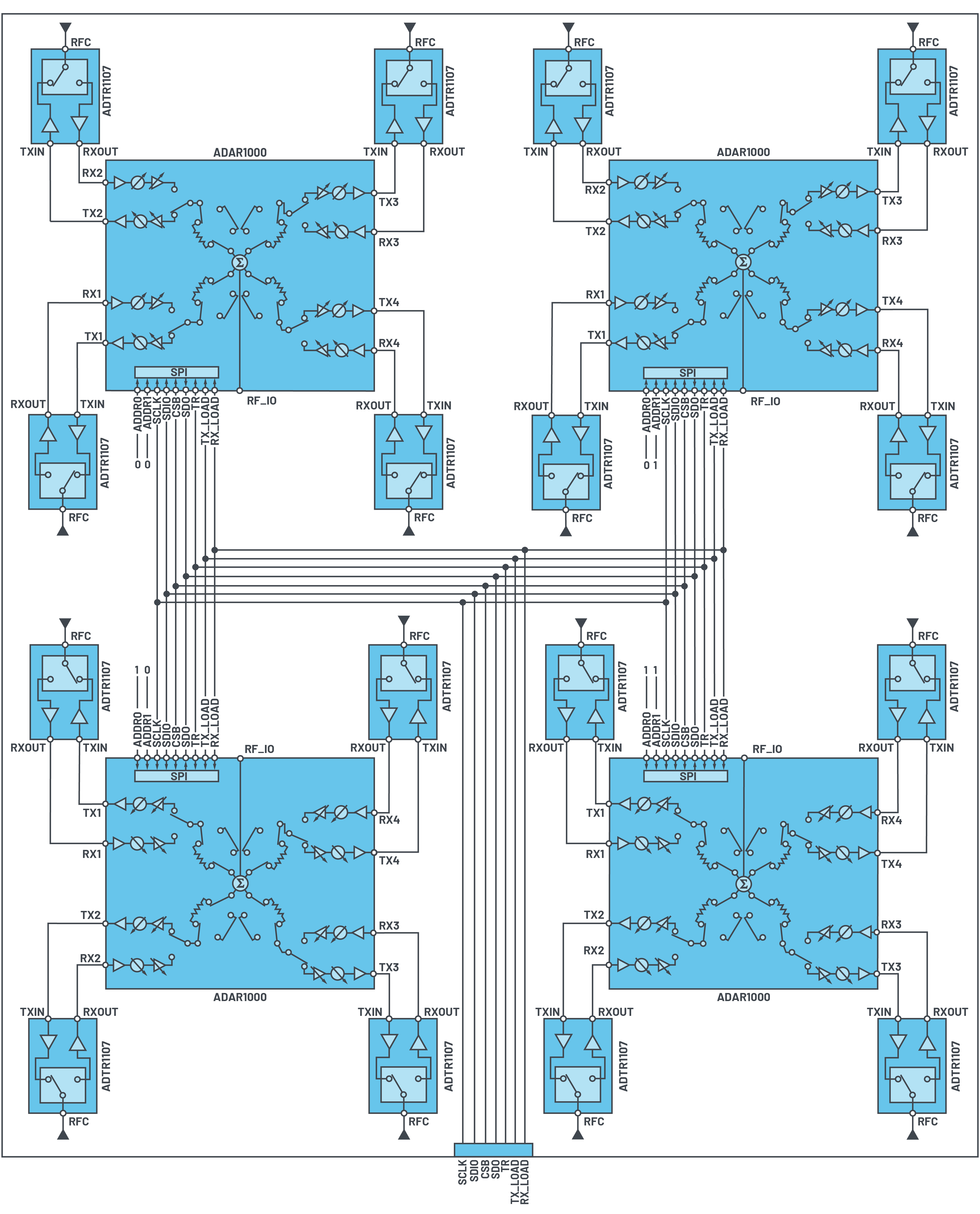
Figure 10. Four ADAR1000 chips driving 16 ADTR1107 chips.

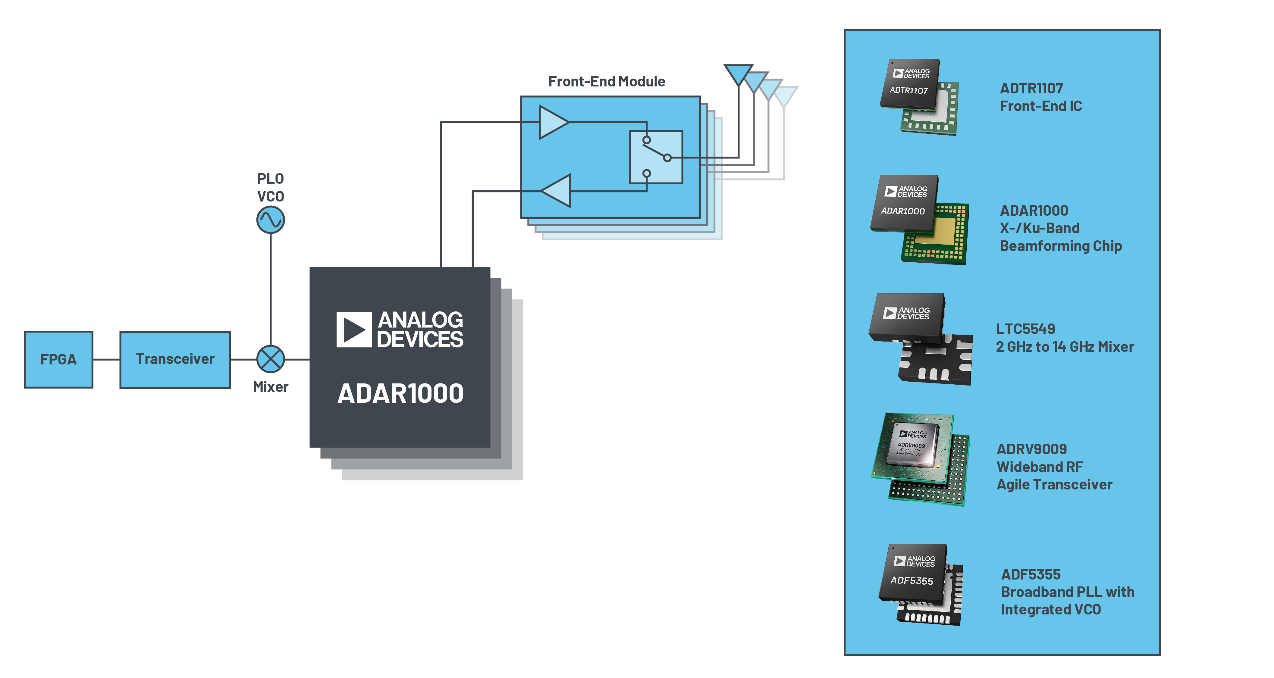
Figure 11. Learn more about ADI’s phased array capabilities at analog.com/phasedarray.
Transceiver Chipsets and Other Companion Products
Highly integrated radio frequency transceiver chips contribute to more integration at the antenna level. The ADRV9009 is an example of such a chip. It offers dual transmitter and receiver, integrated synthesizer, and digital signal processing functions. The device includes a state-of-the-art direct conversion receiver with high dynamic range, wide bandwidth, error correction, and digital filtering built in. Auxiliary functions include an analog-to-digital converter (ADC) and a DAC. General-purpose inputs/outputs for the power amplifier and RF front-end control are also integrated. A high performance phase-locked loop provides fractional-N RF frequency synthesis for the transmitter and receiver signal paths. It offers a very low power consumption and comprehensive power-down modes to further conserve power when not in use. The ADRV9009 is packaged in a 12 mm × 12 mm, 196-ball chip scale ball-grid array.
Analog Devices offers the complete signal chain for phased array antenna design from antenna to bits and has optimized the ICs for this application allowing a faster time to market for our customers. The advancements in the IC technology resulted in a technology shift in antenna designed fueling changes across multiple industries.
Learn more about ADI’s phased array capabilities at analog.com/phasedarray.
About the Authors
Jeff Lane graduated from the University of Massachusetts with an M.S. degree in electrical engineering and has worked for Analog Devices since 2001. His experience includes microwave antenna design, systems engineering, sa...
Related to this Article
Products
RECOMMENDED FOR NEW DESIGNS
6 GHz to 18 GHz, Front-End IC
RECOMMENDED FOR NEW DESIGNS
8 GHz to 16 GHz, 4-Channel, X Band and Ku Band Beamformer
PRODUCTION
2GHz to 14GHz Microwave Mixer with Integrated LO Frequency Doubler
Industry Solutions
Resources
{{modalTitle}}
{{modalDescription}}
{{dropdownTitle}}
- {{defaultSelectedText}} {{#each projectNames}}
- {{name}} {{/each}} {{#if newProjectText}}
-
 {{newProjectText}}
{{/if}}
{{newProjectText}}
{{/if}}
{{newProjectTitle}}
{{projectNameErrorText}}
Latest Media 21


