How Error Vector Magnitude (EVM) Measurement Improves Your System-Level Performance
How Error Vector Magnitude (EVM) Measurement Improves Your System-Level Performance
by
Erkan Acar
Apr 1 2021
Error vector magnitude (EVM) is a popular system-level performance metric that is defined in many communication standards, such as wireless local area networks (WLAN 802.11), mobile communications (4G LTE, 5G), and many more, as a compliance test. Beyond this, it is an extremely useful system-level metric to quantify the combined impact of all the potential impairments in a system through a single and easy to understand value.
Most RF engineers are trained on numerous RF performance parameters, such as noise figure, third-order intercept point, and signal-to-noise ratio. Understanding the combined impact of these performance parameters to the overall system-level performance can be challenging. Instead of evaluating multiple individual performance metrics, EVM offers a quick insight into the overall system. In this article, we will analyze how low level performance parameters impact the EVM and study a few practical examples to put EVM in use to optimize the system-level performance of devices. We will demonstrate how to achieve up to 15 dB lower EVM than what most communication standards target.
What Is Error Vector Magnitude?
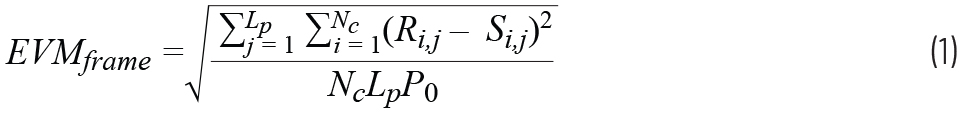
EVM is a simple metric to quantify the combination of all signal impairments in a system. It is frequently defined for devices that use digital modulation, which can be represented through a plot of in-phase (I) and quadrature (Q) vectors also known as a constellation diagram, as shown in Figure 1a. In general, EVM is calculated by finding the ideal constellation location for each received symbol, as shown in Figure 1b. The root means square (rms) of all error vector magnitudes between the received symbol locations and their closest ideal constellation locations constitute the EVM value of the device.1
Equation 1 shows an example EVM formula from the IEEE 802.11 standard.2
where:
Lp is the number of frames, Nc is the number of carriers, Ri,j is the received symbol, and Si,j is the ideal symbol location.

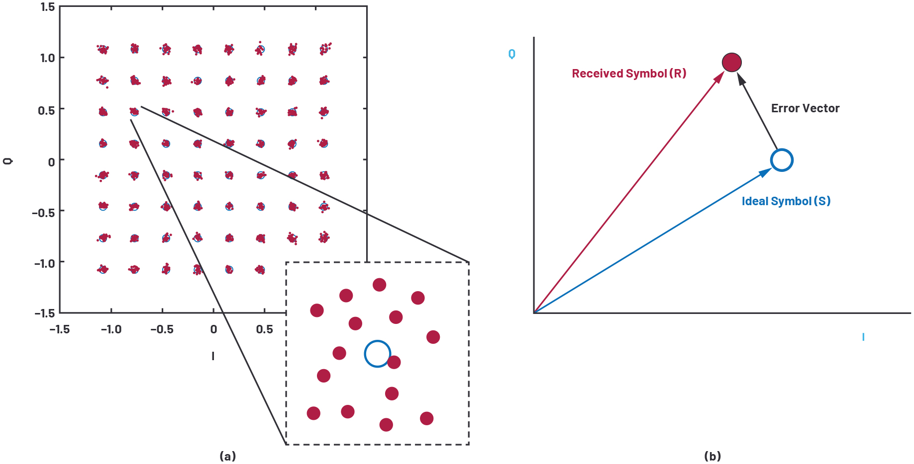
Figure 1. (a) A constellation diagram and a decision boundary, and (b) an error vector between the received symbol and the ideal symbol location.
EVM is closely related to the bit error rate (BER) of a given system. As the received symbols fall far from the target constellation point, the probability of them falling within the decision boundary of another constellation point increases. This translates to a larger BER. One important distinction between BER and EVM is that the BER for a transmitted signal is calculated based on the transmitted bit pattern, while the EVM is calculated based on the distance of the symbol’s closest constellation point and the symbol location. In some cases, symbols may cross the decision boundary and are assigned an incorrect bit pattern. If the symbol falls closer to another ideal symbol location, this may result in a better EVM for that symbol. Therefore, while EVM and BER are closely related, this relationship may not hold for very high levels of signal distortion.
Modern communication standards prescribe a minimum acceptable EVM level based on the transmitted or received signal characteristics, such as data rate and bandwidth. Devices that achieve the target EVM level comply with the standard while the devices that fail their target EVM will be out of compliance. Test and measurement equipment targeted for validation against communication standards typically use a more stringent EVM target, which can be an order of magnitude lower than the target standard. This enables the test and measurement equipment to characterize the EVM of the device under test without significantly distorting the signal.
What Influences EVM?
As an error metric, EVM is closely related to all error sources within a system. We can quantify the EVM impact of all the impairments by calculating how they distort the received and transmitted signals. Let’s analyze the impact of several key impairments, such as thermal noise, phase noise, and nonlinearities, on EVM.
White Noise
White noise exists in all RF systems. When the noise is the only impairment in a system, the resulting EVM can be calculated using the following formula:

where SNR is the signal-to-noise ratio of the system in decibel (dB) and PAPR is the peak-to-average power ratio of a given signal in dB. Note that SNR is typically defined for a single tone signal. For a modulated signal, the PAPR of the signal needs to be considered. Since the PAPR of a single tone signal is 3 dB, this number needs to be subtracted from the SNR value for a waveform with an arbitrary PAPR value.
For high speed converters, such as analog-to-digital converters (ADCs) and digital-to-analog converters (DACs), Equation 2 can be expressed in terms of noise spectral density (NSD):

where NSD is the noise spectral density in dBFS/Hz, BW is the bandwidth of the signal in Hz, PAPR is the peak-to-average power ratio, and Pbackoff is the difference between the peak power of the signal and the full-scale range of the converter. This formula can be very handy to directly calculate the expected EVM of a device using the NSD specification, which is commonly specified for the state-of-the-art high speed converters. Notice that quantization noise also needs to be considered for high speed converter devices. Most high speed converters’ NSD specification also includes the quantization noise. Therefore, Equation 3 represents not only the thermal noise, but also the quantization noise for high speed converters.
As these two equations highlight, the EVM of a signal is directly related to its total signal bandwidth, peak-to-average ratio, and the thermal noise of the overall system.
How Phase Noise Impacts EVM
Another form of noise that influences the EVM of a system is phase noise, which is random fluctuations in phase and frequency of a waveform.3 All nonlinear circuit elements introduce phase noise. The primary sources of phase noise in a given system can be traced back to its oscillators, such as the reference clock, local oscillator (LO), and sampling clocks. Multiple oscillators—such as the sampling clock of a data converter, a local oscillator used for frequency conversion, and a frequency reference—can contribute to the overall phase noise of the system.
Performance degradation due to phase noise is frequency dependent. For a typical oscillator, most of the carrier’s energy is at its fundamental oscillation frequency, which is called the center frequency. A fraction of the signal’s energy would spread around this center frequency. The ratio of the signal’s amplitude in a 1 Hz bandwidth at a specific frequency offset to its amplitude at the center frequency is defined as the phase noise at that specific frequency offset, as shown in Figure 2.

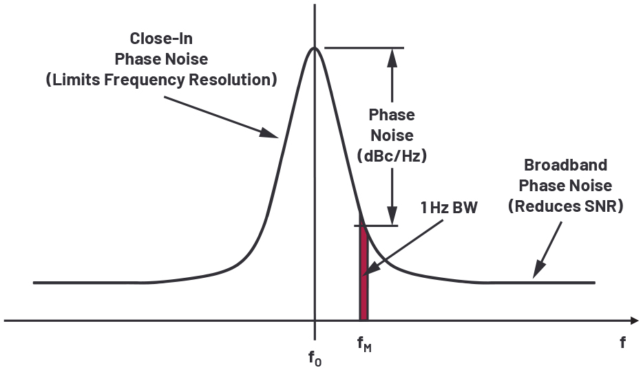
Figure 2. Phase noise.
The phase noise of a system impacts its EVM directly. The EVM due to the phase noise of the system can be calculated by integrating the phase noise over the bandwidth. For modern communication standards that use orthogonal frequency domain modulation (OFDM), the phase noise should be integrated from starting at about 10% of the subcarrier spacing to the total signal bandwidth.

where L is the single sideband phase noise density, fsc is the subcarrier spacing, and BW is the signal bandwidth.
Most frequency generation devices have low phase noise at frequencies <2 GHz, with typical integrated jitter levels orders of magnitude lower than the EVM limits defined in the standards. However, at higher frequencies and with wider signal bandwidths, the integrated phase noise levels can be significantly large, which could lead to much higher EVM values. This is usually the case for millimeter wave (mmWave) devices that operate at frequencies greater than 20 GHz. As we will discuss more in the Design Example section, the phase noise should be calculated for the overall system to achieve the best overall EVM.
Calculating the Impact of Nonlinearities on EVM
System-level nonlinearities lead to intermodulation products, which can fall within the signal bandwidth. These intermodulation products can overlap with the subcarriers, impacting their amplitude and phase. The average error term originating from these intermodulation terms can be calculated. Let’s derive a simple formula to calculate the EVM of a system due to third-order intermodulation products.
As shown in Figure 3a, a two-tone signal will create two intermodulation products. The power of the intermodulation products can be calculated as follows:


where Ptone is the power of the test tone, OIP3 is the output third intercept point, and Pe is the error signal, representing the power difference between the fundamental and the intermodulation product.
For an OFDM signal with N tones as shown in Figure 3b, Equation 6 becomes:

where Pe,i is the error term for each pair of tones.
Since there are N/2 intermodulation products at each subcarrier location that overlap, the equation can be rewritten as:

The total error including all subcarrier locations becomes:

Substituting Equation 6 into Equation 8, the EVM can be expressed as follows:


where PRMS is the rms average of the signal, and C is a constant that ranges from 0 dB to 3 dB depending on the modulation scheme. As Equation 11 shows, EVM decreases as the OIP3 of a system increases. This is expected as a higher OIP3 generally indicates a more linear system. In addition, as the rms power of the signal decreases, the EVM decreases as the power of the nonlinear products decrease.

Figure 3. OFDM intermodulation products.
System-Level Performance Optimization Using EVM
Typical system-level design starts with a cascade analysis where the low level performance parameters of the building blocks are used to determine the overall performance of the system constructed using these blocks. There are well established analytical formulas and tools that can be used to calculate these parameters. However, many engineers do not think how to correctly use cascade analysis tools to design fully optimized systems.
As a system-level performance metric, EVM offers valuable insight to design engineers to optimize their system design. Instead of looking into multiple parameters, the designers can easily choose to optimize the rms value of EVM, thereby achieving an optimum system design.
EVM Bathtub Curve
We can combine the factors into a single plot by considering the EVM contribution of each impairment and the output power level. Figure 4 shows a typical EVM bathtub curve for a system based on the operating power level. At low operating power levels, the EVM performance is dominated by the noise performance of the system. At high operating power levels, the nonlinearities in the system influence the EVM. The lowest EVM level for a system is typically defined by the combination of all the error sources, including phase noise.

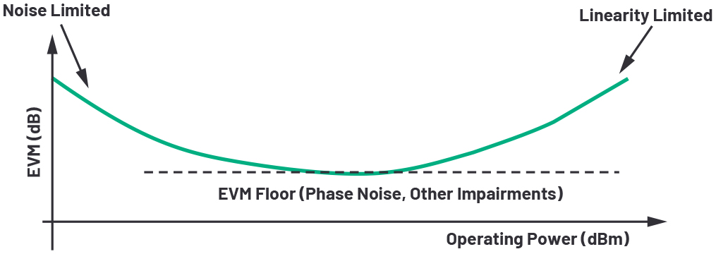
Figure 4. Bathtub EVM curve showing EVM vs. operating power.
We can summarize the total EVM through Equation 12:

where EVMWN is the EVM contribution originating from white noise, EVMPhN is the phase noise contribution, and EVMlinearity is the EVM originating from nonlinear distortion. For a given power level, the power sum of all these error terms indicates the total EVM level in a system.
Along with Equation 12, the bathtub curve of a system can be highly instrumental in system-level optimization where the combination of all the impairments of a given system can be visualized.
Design Example
Let’s design a practical signal chain using EVM as a metric. In this example, we will design a mmWave transmitter using an RF sampling DAC, a mmWave modulator, and mmWave frequency generation devices, and other signal conditioning devices, as shown in Figure 5.

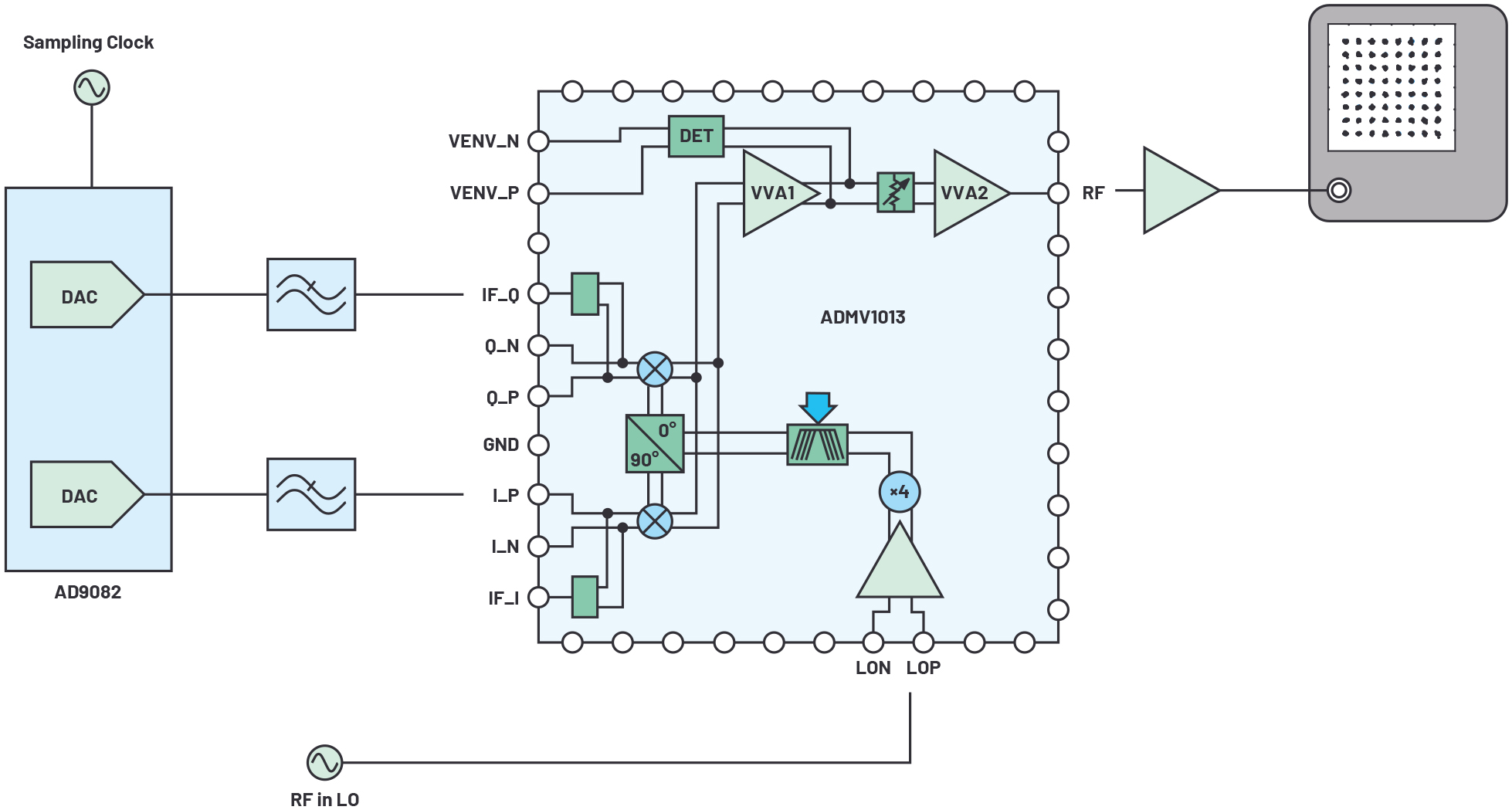
Figure 5. mmWave transmitter signal chain.
This signal chain uses the AD9082 device, which contains quad DACs and dual ADCs with sample rates of 12 GSPS and 6 GSPS, respectively. These direct RF capable converters provide flexibility in the design of the mmWave signal chain and unmatched performance. Figure 6 shows the measured EVM of a typical AD9082 using an AD9213, 12-bit 10 GSPS analog-to-digital converter. The loopback configuration of these two devices shows an EVM level of as low as –62 dB, which is 27 dB lower than the standard limit.

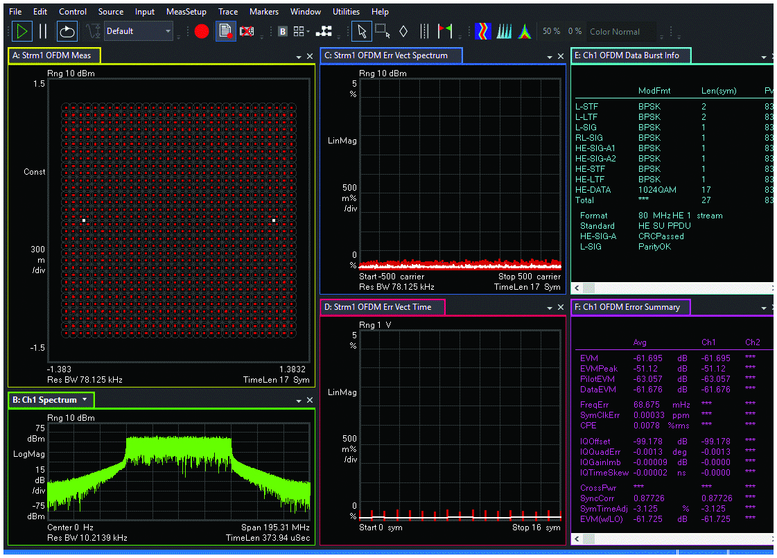
Figure 6. The typical measured EVM of AD9082 using AD9213 at 400 MHz intermediate frequency for an 80 MHz bandwidth IEEE 802.11ax waveform with QAM-1024 modulation.
This signal chain also uses a fully integrated mmWave modulator, ADMV1013, which incorporates numerous sub-blocks of a traditional signal chain, such as frequency multipliers, quadrature mixers, and amplifiers, into a single component. In order to reduce the filtering complexity, we are using the complex IF topology in this design where the quadrature mixers of the modulators are fed with signals that are in quadrature. This eliminates one of the sidebands of the upconverted signal, thereby reducing the filtering complexity compared to a double sideband upconversion operation.
In order to optimize this signal chain to obtain the lowest EVM, we will first analyze the system-level phase noise, then discuss the trade-off between noise and linearity, and finally put all the building blocks together.
Improving EVM by Budgeting for Optimal Phase Noise
As we discussed earlier, the phase noise of the overall system can limit the overall EVM performance at mmWave frequencies. In order to ensure the overall EVM is minimized, let’s analyze the phase noise contribution of each stage to ensure we pick the best components for this signal chain.
The components that create frequencies in this signal chain are the DAC, which is clocked using a synthesizer, and the LO signal. The overall phase noise can be expressed in terms of the following:

where ℒTx is the total phase noise of the transmitter, ℓIF is the phase noise of the DAC output, and ℓLO is the LO signal’s phase noise.
The DAC used in this example, AD9082, has an exceptionally low additive phase noise. The overall phase noise at the output, which is the IF signal, can be calculated using the simple formula shown in Equation 14:

where ℒCLK is the integrated phase noise of the clock signal, fIF is the IF frequency at the output of the DAC, and fCLK is the sampling clock for the DAC. Let’s analyze two candidates for the sampling clock and LO source to ensure we pick components with the lowest phase noise and complexity.
Figure 7 shows the single sideband phase noise of two leading synthesizer candidates for this signal chain. The integrated phase noise for a 5G NR waveform can be calculated by integrating the phase noise of the signal sources using the 6 kHz to 100 MHz integration bandwidth, as shown in Table 1.

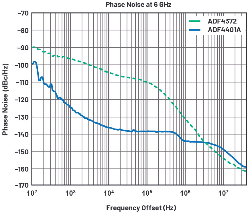
| Component | Integrated Phase Noise @ 6 GHz (dBc/Hz) | Integrated Phase Noise @ 2 GHz (dBc/Hz) | Integrated Phase Noise @ 30 GHz (dBc/Hz) |
| ADF4372 | –54.6 | –64.1 | –40.6 |
| ADF4401A | –73.1 | –82.6 | –59.1 |
At the typical intermediate frequencies for this signal chain, both the ADF4372 and ADF4401A have extremely low integrated noise levels. Since the ADF4372 requires a much smaller overall printed circuit board (PCB) area, it is a good choice to provide the sampling clock for the RF converter, which creates the IF signal. However, as expected, the ADF4401A device becomes the signal generator choice for the LO signal generation due to its inherently low starting phase noise. At 30 GHz, it has about 20 dB lower integrated noise compare to that of the ADF4372 device. This low integrated phase noise level ensures that the LO signal’s phase noise is not limiting the overall EVM performance of the complete system.
Using Equation 13, the overall EVMPhN due to phase noise can be calculated as shown in Equation 15:
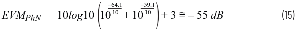
This EVM level due to phase noise is more than enough to measure signals that have ~–30 dB EVM levels as defined by the 5G NR standard.
Trade-Off Between Noise and Linearity
One of the most basic trade-offs in an RF design involves the choice between the noise performance and linearity performance of the overall system. Optimizing for one of these two performance parameters usually leads to a suboptimal performance in the other. System-level EVM analysis can be a very useful tool when it comes to optimizing the performance of the overall system.
Figure 8 illustrates the trade-off between noise and linearity for the signal chain we constructed earlier. Each of the traces are obtained by varying the control voltage of the integrated voltage variable amplifier (VVA). For each trace, the output power level of the DAC has been varied. Notice that as the power level increases, the EVM decreases due to an increase in the overall SNR of the system. After a certain power level, the nonlinearities of the total signal path start degrading the EVM performance. The resulting EVM bathtub curve for a given VVA configuration is very narrow.

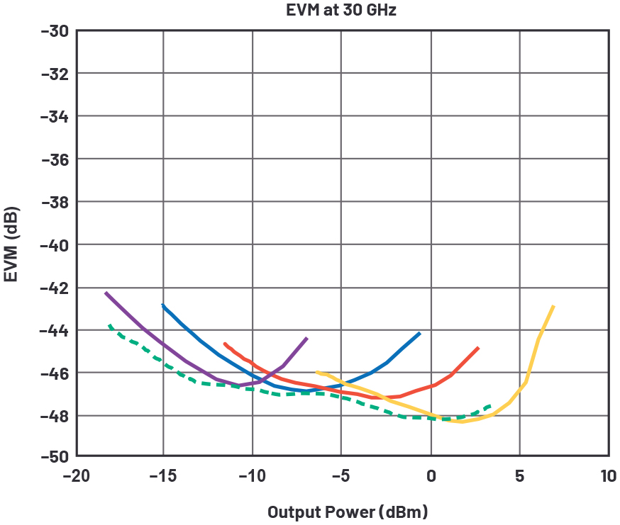
Figure 8. The trade-off between the noise and linearity of the full system.
Luckily, by adjusting the VVA control voltage, we can transition to another curve where the overall system has a lower EVM. The dashed curve in Figure 8 represents the system-level optimization that can be achieved by using the integrated VVAs of the ADMV1013. The resulting bathtub curve after this optimization is much wider, which enables ultralow EVM at a wide range of output power levels.
Conclusion
In this article, we discussed EVM as a system-level performance metric and how to optimize system-level performance through EVM. As we have shown, EVM is a good indicator for many system-level issues. All error sources lead to a measurable EVM, which can be used to optimize the overall performance. We have shown that using the latest high speed converters and fully integrated mmWave modulators, instrumentation-grade performance can be demonstrated and orders of magnitude lower EVM compared to the target communication standard can also be achieved.
About the Authors
Erkan Acar earned both his Ph.D. and M.S. degrees from Duke University in Durham, North Carolina. Erkan has led numerous research and development projects on low cost RF testing, automated test equipment, and signal and po...
Related to this Article
Products
RECOMMENDED FOR NEW DESIGNS
MxFE™ Quad, 16-Bit, 12GSPS RFDAC and Quad, 12-Bit, 4GSPS RFADC
RECOMMENDED FOR NEW DESIGNS
MxFE Quad, 16-Bit, 12 GSPS RF DAC and Dual, 12-Bit, 6 GSPS RF ADC
RECOMMENDED FOR NEW DESIGNS
16-Bit, 12 GSPS, RF DAC and Direct Digital Synthesizer
24 GHz to 44 GHz, Wideband, Microwave Upconverter
Translation Loop, PLL, VCO Module
Microwave Wideband Synthesizer with Integrated VCO
Quad, 16-Bit, 12 GSPS RF DAC with Wideband Channelizers
Dual, 16-Bit, 12.6 GSPS RF DAC and Direct Digital Synthesizer
Industry Solutions
{{modalTitle}}
{{modalDescription}}
{{dropdownTitle}}
- {{defaultSelectedText}} {{#each projectNames}}
- {{name}} {{/each}} {{#if newProjectText}}
-
 {{newProjectText}}
{{/if}}
{{newProjectText}}
{{/if}}
{{newProjectTitle}}
{{projectNameErrorText}}
Latest Media 21


