“Gettin’ In Tune” with the EMI Filter
Abstract
This article presents the analysis and design guidelines for the conventional common-mode/differential-mode passive EMI filter typically implemented in ECG and bioimpedance (BioZ) AFE circuits. Details are illustrated of how an unbalanced EMI filter facilitates common-mode noise bleed into the differential signal path, thereby reducing SNR performance. This is referred to as common-mode to differential-mode conversion (CM-to-DM conversion). Through the judicious choice of components, a designer can mitigate related SNR degradation while providing appropriate signal filtering for ECG and BioZ AFEs.
What You’ll Learn
- Learn how to analyze the transfer function of a CM-to-DM filter.
- Identify noise sources that can potentially corrupt performance in unbalanced filter circuits.
- Gain understanding of common-mode to differential-mode conversion.
- Learn how to set the common-mode filter bandwidth and the differential-mode filter bandwidth.
- Recommended filter settings for use with the MAX3000x ECG and BioZ AFE devices.
Introduction
This article presents an analysis and discussion of the performance limitations due to imbalances in the conventional common-mode (CM)-to-differential-mode (DM) passive filter.
Figure 1 shows the schematic diagram of a typical circuit implementation of the MAX30001 electrocardiogram (ECG) analog front end (AFE). The two external electromagnetic interference (EMI) filters (one highlighted in blue) shown in Figure 1 are conventional CM-to-DM filter circuits.

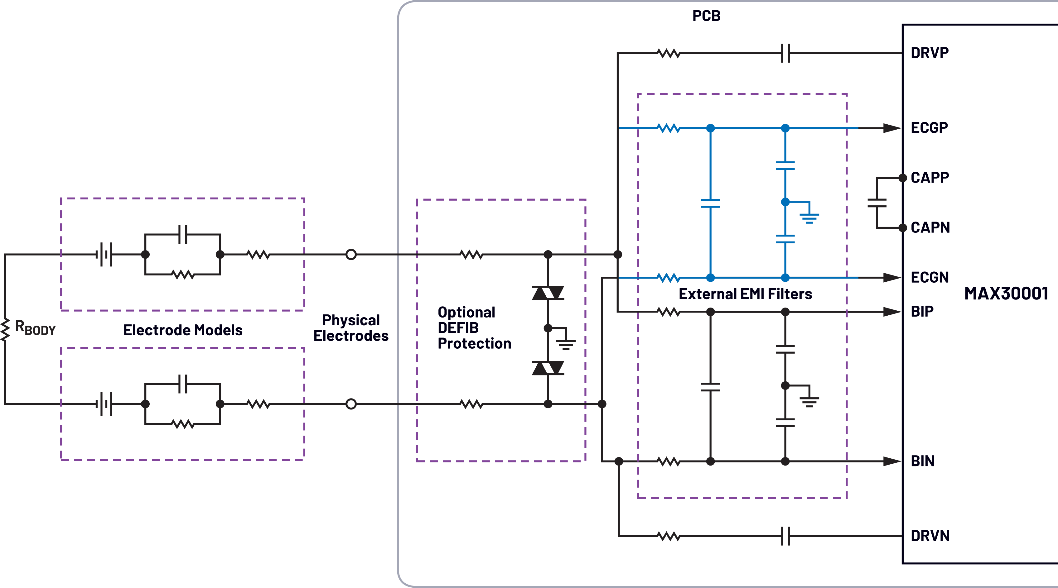
The referenced external EMI filters (implemented with conventional CM-to-DM filter circuits) offer both common-mode and differential-mode bandwidth limiting. Moreover, by judiciously choosing just one component value (the differential mode capacitor), a designer can mitigate signal-to-noise ratio (SNR) degradation due to the imbalance of the common-mode signal path. Not bad for just five passive components!
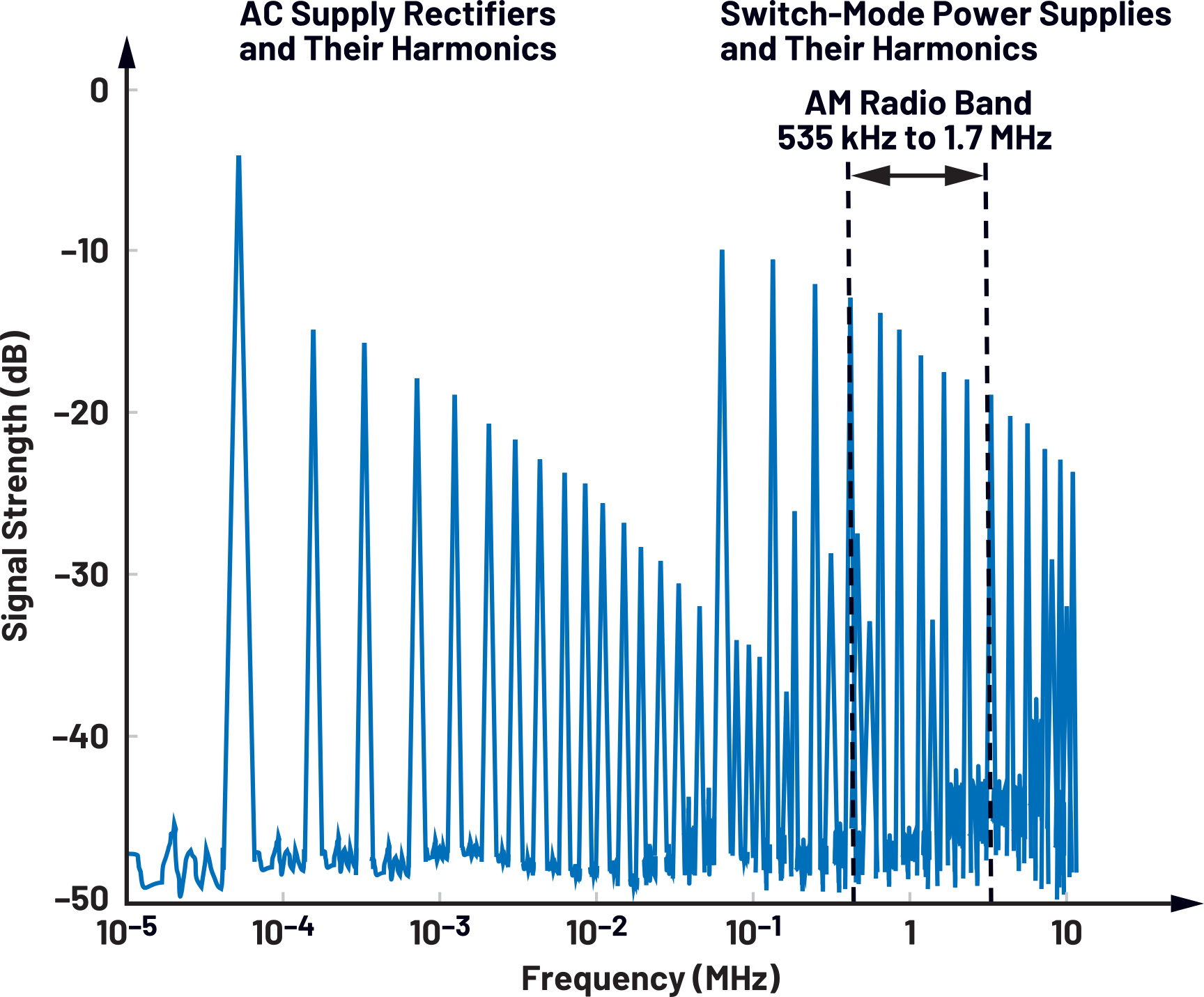
Before diving into this circuit, let’s briefly discuss what external EMI sources can be anticipated. EMI is a circuit disturbance associated with external sources of electromagnetic induction (such as magnetic coupling), electrostatic coupling (such as capacitive coupling), or conduction. Fundamentally, EMI can couple into circuits via radiation and/or conduction. Figure 2 shows the frequency spectra with examples of several common sources of EMI.

The Conventional CM-to-DM Passive Filter
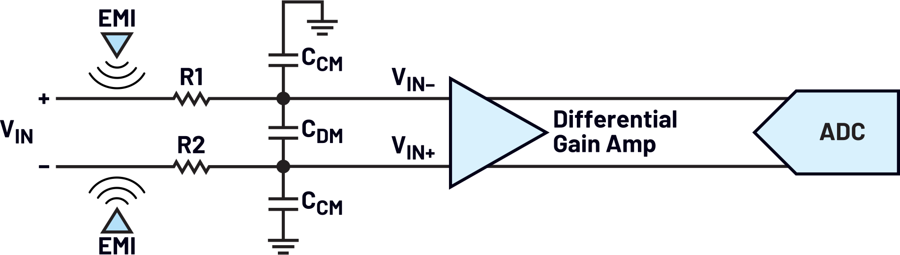
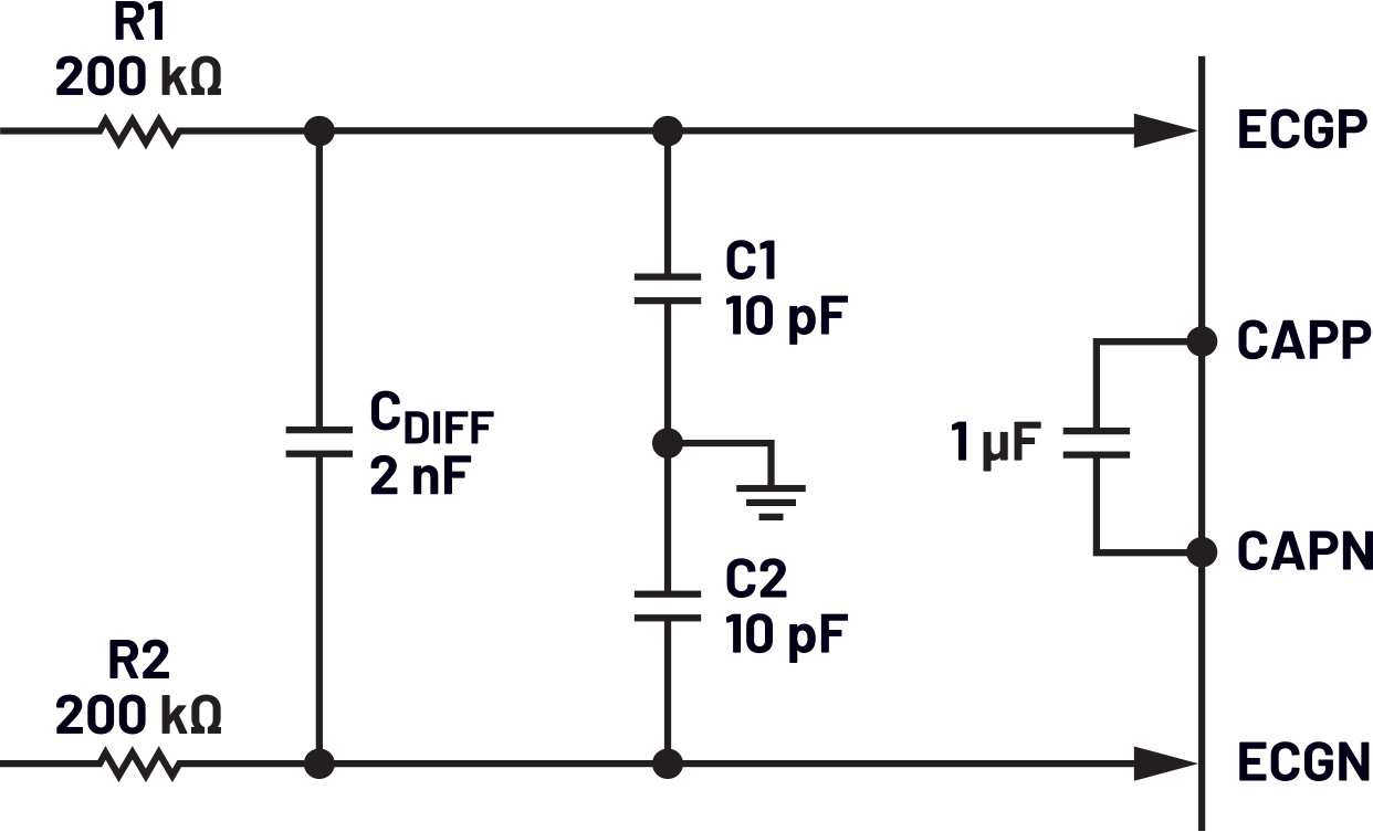
Figure 3 shows the conventional CM-to-DM passive filter typically employed to mitigate environmental noise. For ECG applications where bandwidths are typically bandwidth limited to 256 Hz (512 SPS) or less, AC power line signals (like 50 Hz/60 Hz) typically generate the most intrusive EMI sources. These signals can show up as common-mode signals that we do not want to interfere with the differential signal of interest. If the CM-DM passive filter is unbalanced, unwanted signals (also known as noise) can corrupt the differential signals of interest.

The Common-Mode Filter and CM-to-DM Conversion
The CM-to-DM passive (EMI) filter can be viewed as a composite filter consisting of a common-mode RC filter and a differential-mode RC filter. Figure 4 shows these two filter configurations as standalone circuits. Note that these filter structures, including the CM-to-DM passive filter, are often used as antialiasing filters (AAF) in sampling analog-to-digital circuits such as delta-sigma modulators. Thus, the analysis herein applies to AAF and other differential-signal circuits as well.

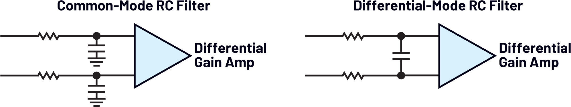
The CM filter is of particular interest as it can be a conduit of noise when its circuit is unbalanced (that is when the two input signal paths have unequal time constants). This is a typical condition given component tolerances, temperature coefficients, voltage coefficients, etc. With an electrical noisy environment, the common-mode rejection of the CM filter will dictate how much noise can potentially get injected into the differential-mode channel. This injected noise will reduce the SNR of the signal of interest (the differential channel signal). This is referred to as CM-to-DM conversion. Anticipating the electrical environment, a designer can apply the appropriate amount of component matching to reduce the CM-to-DM conversion.
Handy Bandwidth Approximations
Before analyzing the CM-to-DM conversion transfer function, let’s calculate the common-mode and differential-mode circuit bandwidths of the balanced CM-to-DM filter first. Not only will these give a designer several handy equations for circuit tuning in ECG/BioZ applications, but they will also aid in the interpretation of the CM-to-DM conversion expression.
Figure 5 shows equivalent circuits for balanced common-mode and balanced differential-mode configurations. In Figure 5a, the balanced common-mode circuit will produce identical signal levels on the output (VOUT = 0 V). Thus, the differential-mode capacitor CDM does not affect the circuit bandwidth and as such is removed from the equivalent circuit model. The common-mode bandwidth is set by the R × CCM time constant.
In Figure 5b, a circuit mirror technique is applied, replacing the differential capacitor with two series capacitors of value 2 × CDM (CDM equivalent impedance). For a balanced circuit, a virtual ground point exists between the 2 × CDM capacitors generating two identical legs, either one setting the bandwidth. The differential-mode bandwidth is set by the R(CCM + 2 × CDM) time constant.

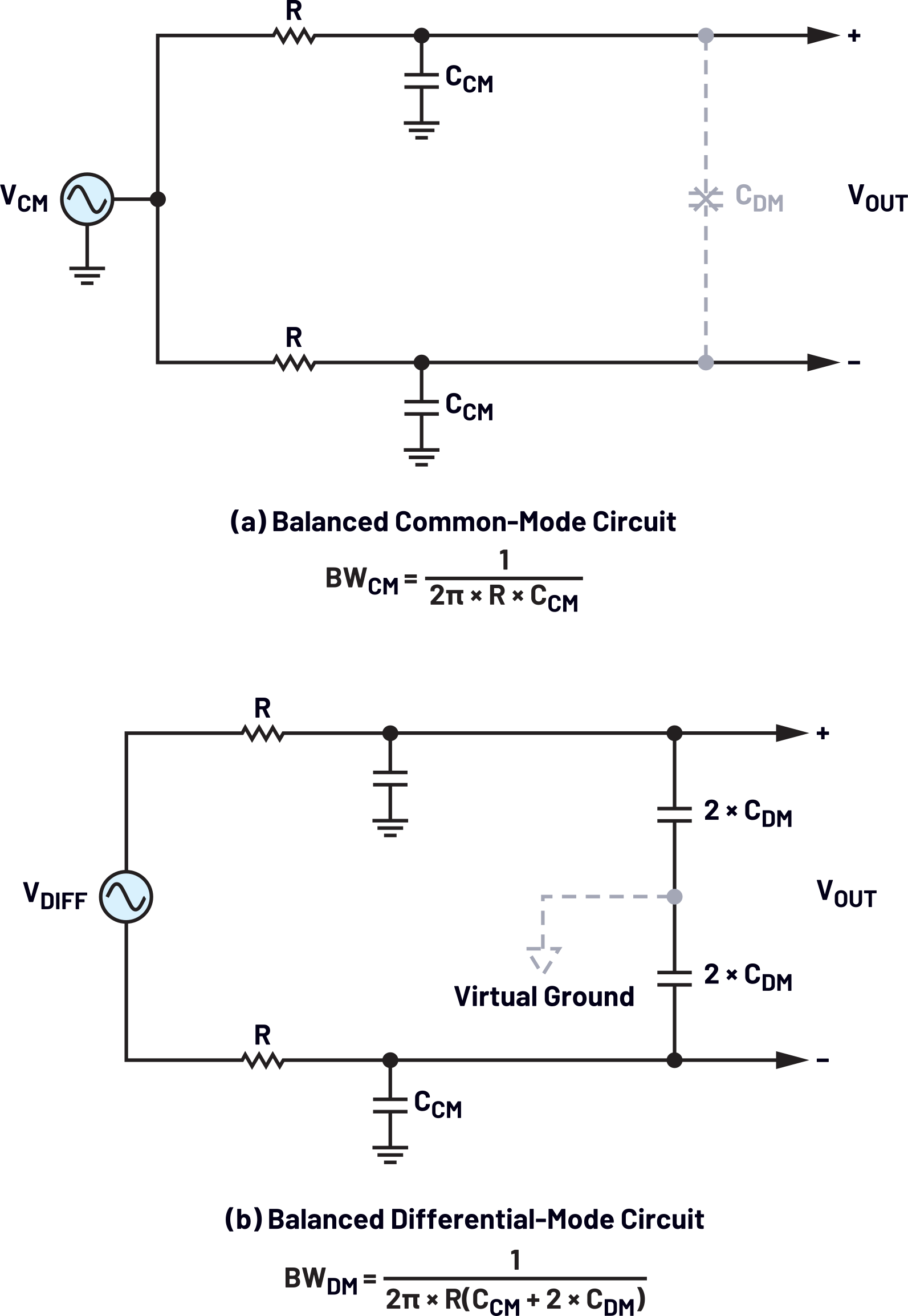
While these handy bandwidth expressions are useful, they are ideal values. Any circuit imbalance will affect the common-mode and differential-mode bandwidths. While an imbalance can lead to a loss of differential signal strength (DM-to-CM conversion), this can be remedied by increasing the gain in subsequent stages. On the other hand, an imbalance with an external noisy environment can lead to a decrease in the differential channel SNR via CM-to-DM conversion.
The CM-to-DM Conversion Transfer Function
Figure 6 shows an equivalent topology for the CM-to-DM circuit analysis: a bridge circuit.

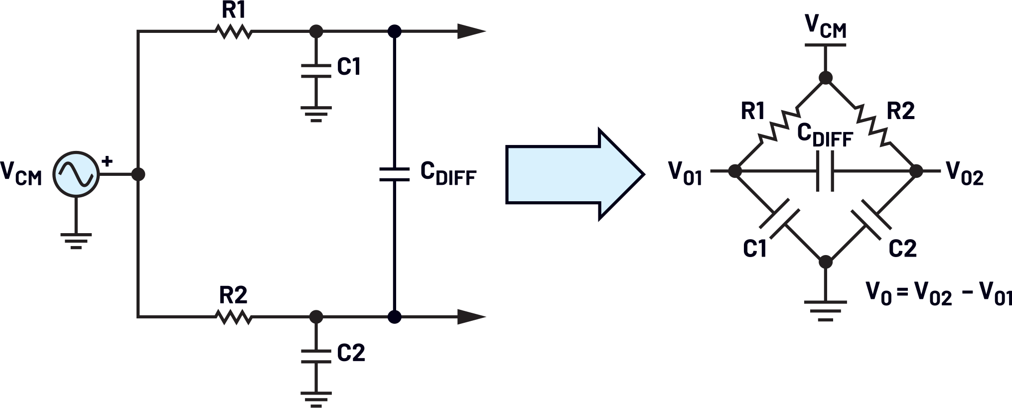
Bridge circuits (for example, Wheatstone Bridge) have been widely used since the mid-nineteenth century. While implemented in a multitude of applications, it is used here as an analysis aide. Figure 7 highlights the transfer function equations for a generic bridge circuit (extended from a Wheatstone bridge derivation).
Applying these equations to the circuit in Figure 6 yields the following CM-to-DM conversion transfer function:
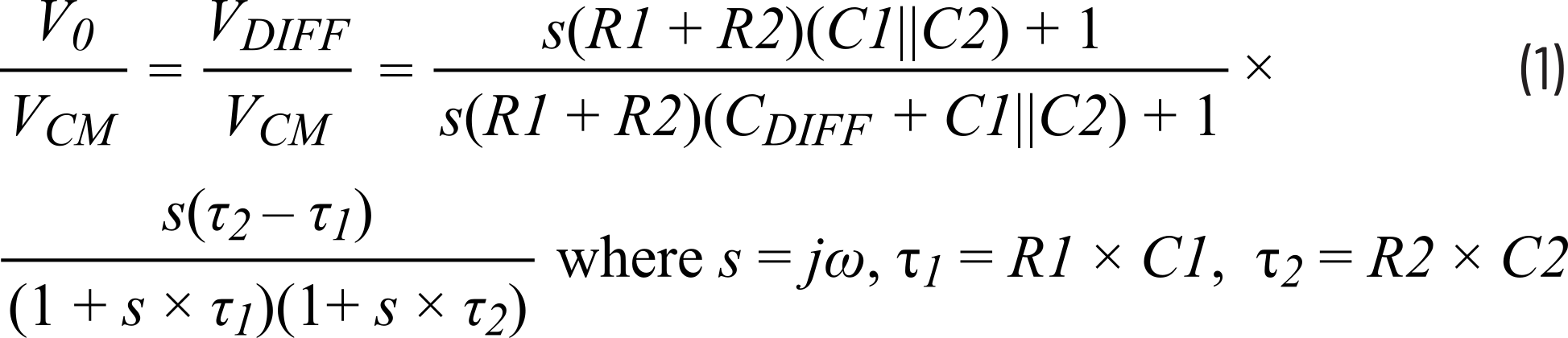
Note that there are three poles and two zeros in this transfer function. From a systems engineering point of view, this is a 3-order, Type 1 system transfer function. Equation 2 displays the generic equation form that highlights the effect of a circuit imbalance (that is when τ2 ≠ τ1).
Surprisingly, this 5-term transfer function is fairly complex for just five passive components. Reviewing the individual terms can help add some insight for potential simplification. Poles p1 and p2 will set two higher frequency corners, where pole p0 will set a lower frequency corner. By default (due to the additional capacitance), BWp0 < BWp1 ≈ BWp2. If a large CDIFF is implemented (CDIFF >> C1||C2), the lower frequency (that is, < BWp0) common-mode noise transfer will be desensitized to the C1 and C2 mismatch.
Handy CM-to-DM Transfer Function Approximations
Referring to the bandwidth approximations from Figure 5, notice that poles p1 and p2 correspond to the common-mode bandwidth. Additionally, if R1 ≈ R2 and C1 ≈ C2, pole p0 corresponds to the differential-mode bandwidth (math left to the reader).
Taking this a little further, if R1 ≈ R2 and C1 ≈ C2, the Z1 zero approximates either of the two poles, p1 and p2. Cancelling an approximate equal pole/zero pair will not only simplify our expression but yield a useful transfer function approximation.
The cancelled pole/zero pair does not affect the CM-to-DM gain at low frequencies. It does add some gain error at higher frequencies (≥ 535 kHz for AM radio emissions) depending on the EMI filter mismatch.
The approximate CM-to-DM conversion transfer function is:
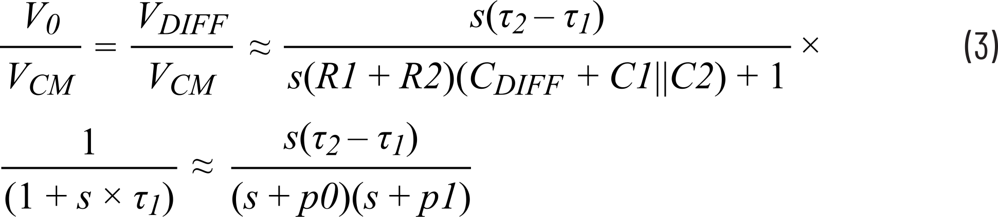
Note: The p1 pole was kept in the expression assuming it sets a higher corner frequency compared to the p2 pole. This pole will have a larger influence on higher frequency attenuations.
Inspection of Equation 3 reveals that when the two time constants in the numerator are equal, the circuit is perfectly balanced and the transfer gain is zero (infinite common-mode rejection). While theoretically possible, this is a very unlikely event. Even if one were to hand balance the circuit, many other effects would cause it to drift from this ideal case (aging, temperature, voltage effects, etc.). A better use of the designer’s time is to understand the sensitivity of the CM-to-DM conversion to component tolerances. This will aid in setting the initial rejection levels for common-mode EMI noise.
Note: The CM-to-DM EMI filter is typically not considered a precision circuit. It is implemented in situations where the environmental noise signal strength is not known well. As such, it is intended to help suppress commonly known noise sources (such as power line disturbances, AM radio disturbances, etc.).
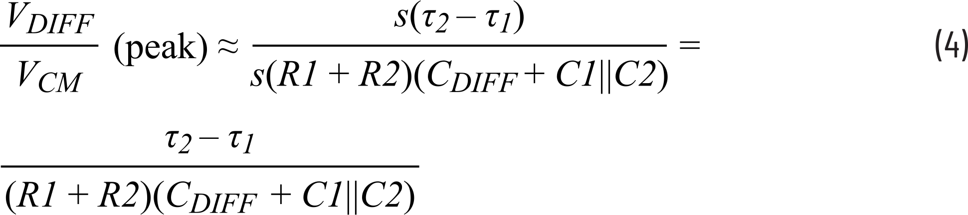
Now that we have crossed the infinity bridge, let’s rejoin the real world and move forward knowing that an imbalance is the norm. In fact, the worst case imbalance is what we concentrate on. Revisiting Equation 3, note the that the transfer function rolls up at 20 dB/dec, flattens out at the lower frequency pole (fL), and then starts to roll down at −20 dB/dec above the upper frequency pole (fH). The center frequency can be approximated by taking the geometric mean of the two pole frequencies. However, this approximation error increases with the component mismatch. For large mismatch errors (such as ±1% tolerance resistors and ±20% tolerance capacitors), it is recommended to find (by hand analysis and/or simulation) the peak gain at −180° phase shift.
The peak mid-frequency gain can be approximated as follows:
If CDIFF >> C1 ≈ C2, the peak mid-frequency gain can be further simplified as follows:

If the same tolerance, denoted by δ, is selected for all the components, Equation 5 reduces to:
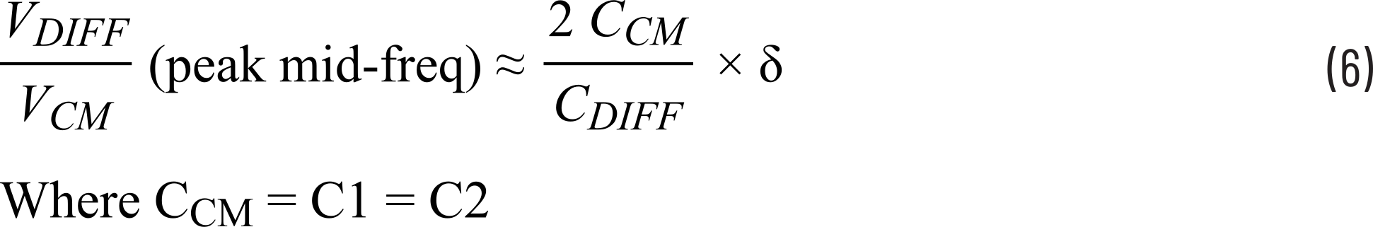
While this is somewhat restrictive from a design point of view (selecting components of equal tolerances), it emphasizes the point that the smaller the capacitor ratio (common-mode to differential-mode capacitance ratio), the greater the circuit attenuates common-mode noise.
Returning to Equation 5, when analyzing the circuit for worst-case tolerance conditions, the values of the components are assumed to be biased such that the numerator is maximized. The larger the mismatch in RC time-constants (circuit unbalance), the more the common-mode noise will bleed into the differential channel. Turning our attention to the denominator term, the expression can be simplified noting that the sum of the resistors will simply be twice the nominal resistance as follows:

Substituting Equation 7 into Equation 5 yields:

Equation 8 is a very simple and handy approximation for the CM-to-DM conversion mid-frequency gain: the common-mode time constant mismatch divided by the nominal differential-mode time constant. As long as CDIFF is large (CDIFF ≥ 100 × (C1 and C2), Equation 8 is quite accurate.
One might be tempted to arbitrarily increase CDIFF to decrease the sensitivity of the numerator (that is, the RC time-constant mismatch). Unfortunately, this is limited as it sets the differential-mode channel bandwidth (the signal of interest). Thus, a trade-off will be required.
The common-mode rejection at 50 Hz/60 Hz (potential power line interference) and 535 kHz (the low end of the potential AM radio spectrum interference) can now be approximated using the peak mid-frequency gain and the lower and upper frequency corners. The following example highlights this.
A CM-to-DM Conversion Transfer Function Example

Let’s assume every component has a 0.1% tolerance. This will give a reference level to compare alternate EMI filter circuit scenarios with (Figure 8). For a worst-case (wc) rejection approximation, use the following values:
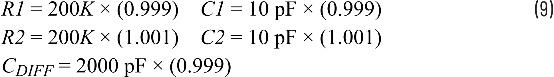
Applying Equation 8,
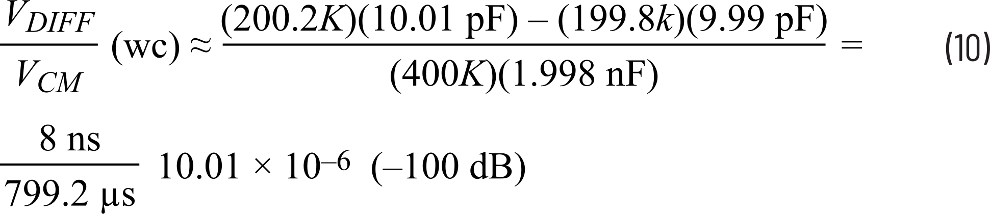
Noting that the denominator of the previous expression is the time constant of the lower frequency corner, we can easily calculate fL:

Now use the smaller RC time constant that sets the higher frequency pole:

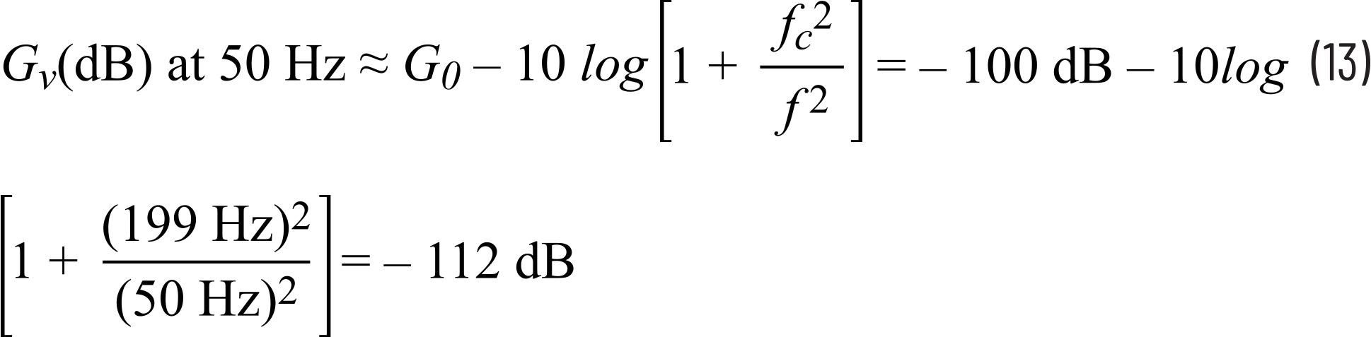
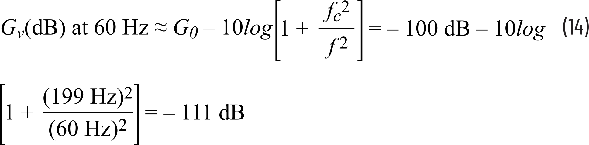
With these values, we can now estimate the attenuation at 50 Hz/60 Hz and 535 kHz as follows:
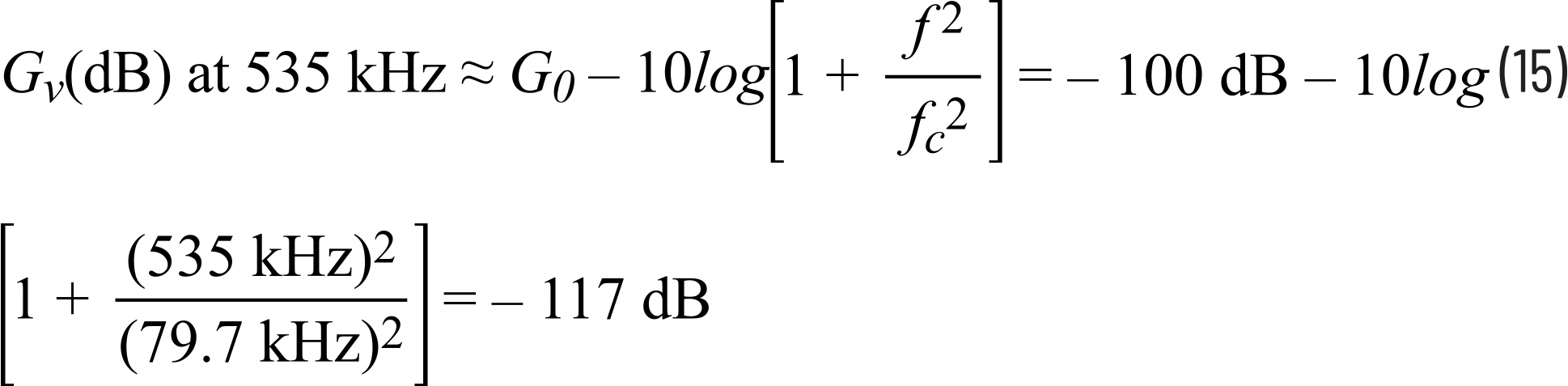
These hand calculations agree well with the circuit simulation (see Figure 9). Remember that this is not intended to be a precision circuit. Approximations within several dB are usually acceptable for an EMI filter application.

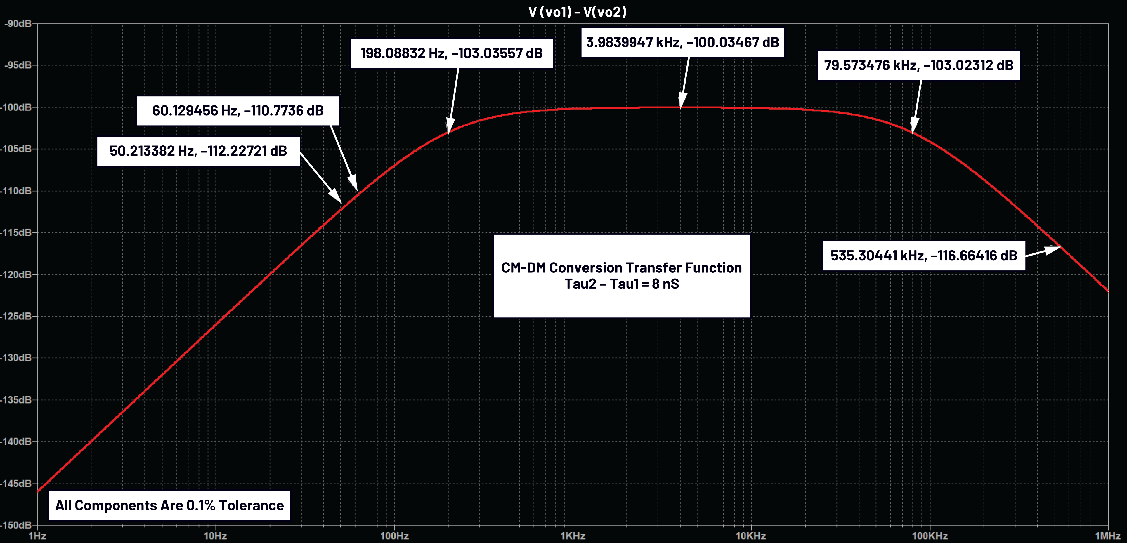
Table 1 highlights this circuit’s CM-to-DM rejection at 50 Hz/60 Hz and 535 kHz for various component tolerance levels. The first scenario (±0.1% tolerance) is a somewhat arbitrary reference-point based on hand-measuring passive components on a lab bench. The other scenarios reflect common commercially available resistor and capacitor tolerance levels for comparison.
| Worst-Case CM-to-DM Attenuation Estimates | ||||||
| Rejection Estimates (Equation 4—Hand Calculation) | EMI Filter Attenuation (LTspice Sim Results) | |||||
| Scenario | Gv (dB) at 50 Hz | Gv (dB) at 60 Hz | Gv (dB) at 535 kHz | Gv (dB) at 50 Hz | Gv (dB) at 60 Hz | Gv (dB) at 535 kHz |
| All Components 0.1% | −112.3 | −110.8 | −116.6 | −112.3 | −110.8 | −116.7 |
| All Res Are 1% and Caps Are 0.1% | −97.5 | −96.0 | −101.7 | −97.4 | −96.0 | −101.9 |
| All Components 1% | −92.3 | −90.8 | −96.4 | −92.2 | −90.8 | −96.6 |
| All Res Are 1% and Caps Are 5% | −82.7 | −81.2 | −86.2 | −82.7 | −81.2 | −86.7 |
| All Res Are 1% and Caps Are 10% | −77.4 | −75.9 | −80.0 | −77.4 | −75.9 | −81.0 |
| All Res Are 1% and Caps Are 20% | −71.7 | −70.2 | −72.3 | −71.7 | −70.2 | −74.3 |
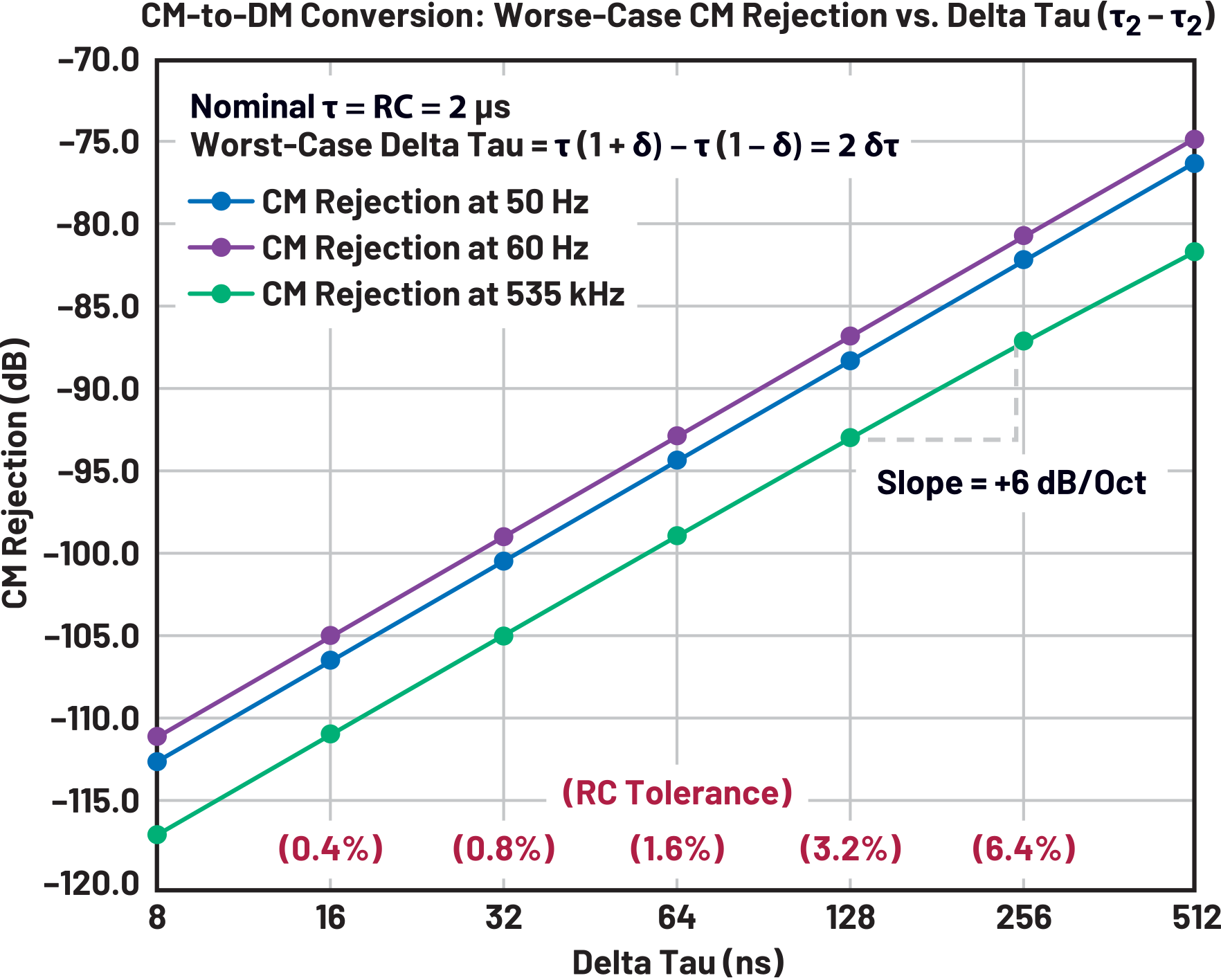
Note that the tolerance of the RC time constant is doubled for a worst-case estimate. That is, if one side of the differential circuit is up X percent, the other side can be down by X percent. For example, if R1 and R2 are 1% tolerance components and C1 and C2 are 10% tolerance components, the worst-case RC time constant mismatch is 22%. A 440 ns (22%) mismatch will decrease the common-mode rejection by 35 dB compared to the 0.1% tolerance reference (that is an 8 ns time constant mismatch). That’s quite a bit of loss! Depending on the use-case environment, this may or may not be acceptable.
Figure 10 displays a plot of the common-mode rejection vs. delta tau, where delta tau is the RC time-constant mismatch. Several corresponding RC tolerance levels are highlighted in red next to the bottom horizontal axis. For clarification, the 64 ns delta tau level corresponds to 1.6% RC tolerance (64 ns/2 µs = 3.2% worst-case mismatch = ±1.6% RC tolerance). Focusing on the slopes of the plot, the common-mode rejection gets 6 dB worse for every doubling of the RC time-constant mismatch.

Summary of Key Points
- Predict and verify your EMI environment.
- The equivalent CM-to-DM circuit is a bridge circuit, which is nonlinear.
- With an appropriate selection of CDIFF, a designer can easily approximate the CM-to-DM conversion using Equation 8 and calculated corner frequencies.
- Making CDIFF large will desensitize the C1 and C2 mismatch, as well as delta tau (that is, the common-mode RC time-constant mismatch).
- To a first-order approximation, the common-mode rejection will decrease by 6 dB for every doubling of RC mismatch.
- Component manufacturing tolerances are only part of the equation. Temperature, voltage, and aging will also influence the component mismatch.
- All calculations are based on worst-case mismatches. Anything else just makes things better, eventually reaching infinite common-mode rejection.
- Analyze and understand your circuit identifying performance trade-offs and applicable approximations. Don’t design by simulation.
- This analysis can be extended to AAF design applications.
Tuning the EMI Filter for ECG Applications
The design of the EMI filter for ECG applications starts with setting the differential-mode signal bandwidth. Fitness use-cases typically target heart rate R’-R’ measurements that can be implemented with a lower bandwidth (40 Hz), whereas arrhythmia detection applications require a higher bandwidth (256 Hz).
For this example, a 256 Hz bandwidth EMI filter will be implemented for arrythmia detection applications. The resistor values have a minimum limit based on IEC 60601-1 safety compliance. Specifically, a single-fault condition must be limited to 50 µA DC for patient protection. Thus, if the ECG AFE IC (such as the MAX30001, MAX30003, MAX30005, MAX86176, or MAX86178) is powered by 1.8 V, the minimum resistor value shall be 36 kΩ (1.8 V/50 µA).
Before choosing the resistor value, a relook at Equation 5 is warranted. The CM-to-DM conversion can be decreased by increasing the denominator (increasing the resistance while holding the CDIFF to CCM ratio constant). While this allows for some design freedom, resistors generate Johnson thermal noise, which can introduce differential signal error. To minimize this noise source, resistor values lower than MΩs are recommended.
Setting our design targets as follows:
Differential-mode channel BW = 282 Hz (allow for 10% tolerance from nominal 256 Hz).
Common-mode channel BW = 48.2 kHz (allow for 10% tolerance from nominal 53.5 kHz, a decade below the lowest AM radio band of 535 kHz).
Note: The initial tolerance assumptions are just starting points assuming the common-mode RC time constants have an approximate 10% tolerance.
With 10 pF caps and a fc = 48.2 kHz, the resistance value calculation shall be 330.2 kΩ.
Calculating the CDIFF value from the differential-mode BW equation given in Figure 5 yields 851.3 pF.
Choose a 330 kΩ, 0.1% tolerance resistor value. The higher accuracy (tolerance) is recommended for better common-mode rejection. The common-mode capacitors can be desensitized by the judicious choice of the differential capacitor value. Thus, the two common-mode capacitors can have a larger tolerance with an associated cost savings.
Note: When dry electrodes are used for ECG measurements, the implementation of the EMI filter is generally discouraged. This is because the EMI filter offers a lower impedance path to the higher impedance of the dry electrode/tissue interface. Basically, the EMI filter bypasses the high common-mode rejection of the instrumentation amplifier in the AFE device. Without extreme matching over all environmental conditions, the EMI filter can degrade the overall system common-mode rejection performance.
Unfortunately, the calculated resistor and capacitor values do not always match up with commercially available components. Thus, the designer needs to research and select the nearest component values that can be obtained based on size, cost, tolerance, tempco, voltage stress, aging, etc. The analysis herein only considers the effects of nominal manufacturing tolerance examples. It is recommended that the designer analyze their use-case thoroughly to adequately capture all associated variances.
Selecting the following EMI filter design components:
R1 = R2 = 330 kΩ, 0.1%; C1 = C2 = 10 pF*, 10%; CDIFF = 850 pF, 10%
*Using lower value capacitors is not recommended due to stray PCB capacitances.
Using Equation 8 and the formula to calculate the attenuation on the first-order roll-up and roll-down skirts yields the following circuit characteristics:
BW (CM) ≈ (2π × (330 k)(10 pF))–1 = 48.2 kHz nominal; BW (Tol) range: 43.8 kHz to 53.6 kHz
BW (DM) ≈ (2π × (330 k)(10 pF + 2 × 850 pF))–1 = 282 Hz nominal; BW (Tol) range: 257 Hz to 313 Hz
WC CM rejection at 50 Hz = –74 dB
WC CM rejection at 60 Hz = –72 dB
WC CM rejection at 535 kHz = –78 dB
A spice simulation was used to validate the above calculations (math and simulations left to the reader). For the worst-case scenario, LTspice® simulation gave the following results:
fH = 49 kHz and fL = 311 Hz
WC CM rejection at 50 Hz = –74 dB and WC CM rejection at 60 Hz = –72 dB
WC CM rejection at 535 kHz = –78.6 dB*
*As previously mentioned, the cancellation of the pole/zero terms will introduce some error to the high frequency attenuation approximation. In this case, our estimate is off by 0.6 dB at 535 kHz.
Note that the rejection levels can be improved by implementing tighter tolerance capacitors. This may be warranted given that the fact that the EMI filter may be setting the common-mode rejection of the front-end electronics, essentially bypassing the FE amp’s CM rejection.
Tuning the EMI Filter for BioZ Applications
The design of the EMI filter for BioZ applications also starts with setting the differential-mode signal bandwidth. However, BioZ involves the injection of AC signals into body tissue where the return signal is analyzed for both magnitude and phase information. Thus, any phase distortion from the filter will introduce signal error.
To avoid phase distortion, it is recommended to set the differential-mode corner frequency several decades higher than the drive frequency. The MAX30001 BioZ circuit provides a 125 Hz to 131.072 kHz injection signal range. Since the differential-mode bandwidth cannot be larger than the common-mode, this sets the frequency corner at 535 Hz while implementing the common-mode corner frequency at 53.5 kHz nominally (a decade lower than the AM radio band).
Setting our design targets as follows:
Differential-mode channel BW = 595 Hz (allow for 10% tolerance from nominal 535 Hz).
Common-mode channel BW = 48.2 kHz (allow for 10% tolerance from nominal 53.5 kHz, a decade below the lowest AM radio band of 535 kHz).
Note: The initial tolerance assumptions are just starting points assuming the common-mode RC time constants have an approximate 10% tolerance.
With 10 pF caps and a fc = 48.2 kHz, the resistance shall be 330.2 kΩ.
Calculating the CDIFF value from the differential-mode BW equation given in Figure 5 yields 400 pF.
Selecting the following EMI filter design components:
R1 = R2 = 330 kΩ, 0.1%; C1 = C2 = 10 pF*, 10%; CDIFF = 400 pF, 10%
*Using lower value capacitors is not recommended due to stray PCB capacitances.
Using Equation 8 and the formula to calculate the attenuation on the first-order roll-up and roll-down skirts yields the following circuit characteristics:
BW (CM) ≈ (2π × (330 k)(10 pF))–1 = 48.2 kHz nominal; BW (Tol) range: 43.8 kHz to 53.6 kHz
BW (DM) ≈ (2π × (330 k)(10 pF + 2 × 400 pF))–1 = 595 Hz nominal; BW (Tol) range: 542 Hz to 661 Hz
WC CM rejection at 50 Hz = –73.6 db
WC CM rejection at 60 Hz = –72.2 dB
WC CM rejection at 535 kHz = –71.2 dB
A spice simulation was used to validate the above calculations (math and simulations left to the reader). For the worst-case scenario, LTspice simulation gave the following results:
FH = 49 kHz and FL = 311 Hz
WC CM rejection at 50 Hz = –73.6 dB and WC CM rejection at 60 Hz = –72 dB
WC CM rejection at 535 kHz = –72 dB*
*As mentioned before, the cancellation of the pole/zero terms will introduce some error to the high frequency attenuation approximation. In this case, our estimate is off by 0.8 dB at 535 kHz.
Some Final Thoughts on the EMI Filter for BioZ Applications
When designing the EMI filter for BioZ applications with higher injection signal frequencies (greater than 535 Hz), the AM radio band common-mode rejection will be diminished. Moreover, higher BioZ injection frequencies will drive designs with lower resistor values. Using a 36 kΩ resistor, our calculated value for IEC 60601-1 safety compliance with a 1.8 V power supply, sets a common-mode bandwidth around 440 kHz with 10 pF caps. Setting the differential-mode corner frequency two decades lower limits the injection frequency to around 4 kHz. Higher BioZ injection frequencies (like the MAX30001 maximum injection frequency is 131 kHz) will require lower resistor values.
CMRR vs. CM-to-DM Conversion
CMRR and CM-to-DM conversion are inverses of each other. CMRR is a positive term (normally) and the CM-to-DM conversion transfer function is the circuit gain that is typically less than 1 V/V (a negative dB value). Noting that the gain terms in the CMRR expression are just ratios of the output to input signals, the CMRR expression can be rearranged to illustrate this relationship in Equation 16.
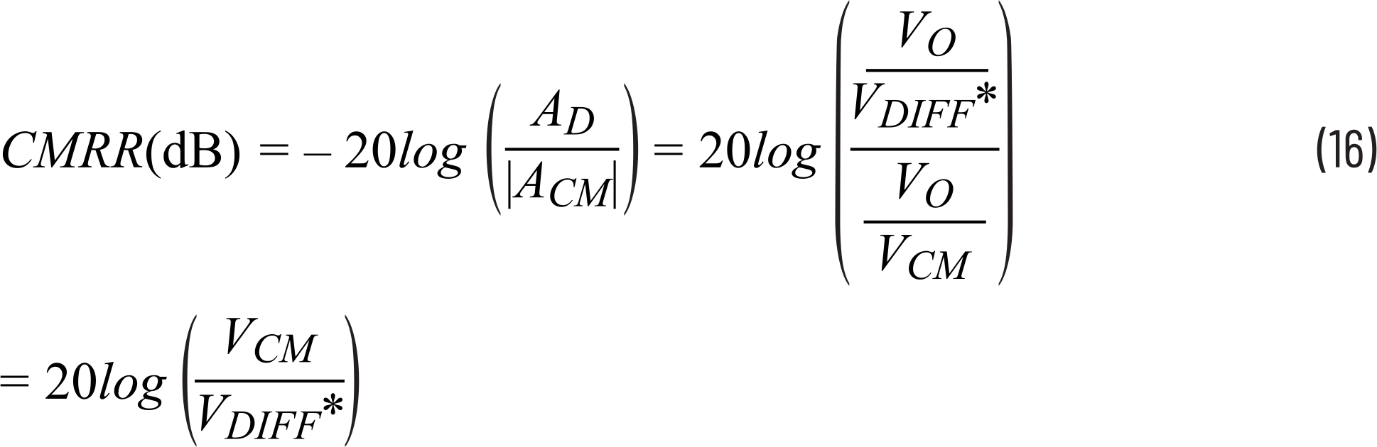
*This is VDIFF, RTI (referenced to input).
The CMRR is a great metric for comparing alternate circuits to each other. While it has its place, it does not directly address the CM-to-DM conversion behavior that occurs within the transfer function of the EMI filter circuit. In this light, the analysis herein is a better vehicle to evaluate and explain the ramifications of an unbalanced EMI filter.
Conclusion
This article discusses knowledge of what the conventional CM-to-DM filter can be used for, what it does, and what it cannot do. Keeping calculations and simulation plots to a minimum, the emphasis has been on an interpretation of the mathematical model for an unbalanced EMI filter. Additionally, equations were simplified where appropriate, stressing handles that the designer can use to their advantage.
It’s amazing how such a simple little circuit with just five passive components can offer such complexity (when unbalanced).
Acknowledgments
The author would like to thank Dan Burton and Fahad Masood for their review and constructive critique of this document.
About the Authors
Related to this Article
Products
Ultra-Low Power, Single-Channel Integrated Biopotential (ECG, R to R Detection) AFE
Ultra-Low-Power, Optical PPG and Single-Lead ECG AFE
Resources
Latest Media 21


