Fiber Optic Systems Get Thermal Enhancements
Background
The global market for fiber optic systems is large. Estimates vary, but many forecasts place it somewhere between $4B to $4.5B in 2019, with a CAGR of close to 10% through 2021. Fiber optics are predominantly used in communications applications such as those found in telecom, home utility, CATV, military, and industrial environments. Fiber optic-based communication has many advantages over other technologies, such as cable, including increased bandwidth, electromagnetic interference immunity, electrical isolation, data security, decreased cost, size, and weight, and low attenuation rates. Growth is fueled by these advantages, but mainly by the need for higher bandwidth communications in consumer and healthcare sectors, as well as government funding for the development of its own network infrastructure.
Taking a closer look at what is driving these promising growth projections, it is clear that it is not just one single trend, but a combination of factors. These include a combination of increasing investments and research being done by the major fiber optic cable manufacturers within the industry to develop and upgrade fiber optic technology. Fiber optic technology has had continuous research and development activities over the past few years, leading to its current prominence and the rising demand for high bandwidth fiber optic cable for communications and data services. This includes fiber optic connectors, sensors, fiber optic broadband, and fiber optic cables.
At the same time, the demand for high speed, bandwidth intensive, high data rate applications has altered the global fiber optics market. New fiber network deployments will be the main driver of the fiber market over the next five to seven years. An optical fiber system typically consists of a myriad of components such as transmitters, receivers, and optical cables. Furthermore, system installations are labor intensive; especially so if they are for underground and undersea connections. However, it is this wide range and diversity of applications that is driving the global fiber optics market; thereby enabling its significant growth rate.
The growing demand for cost-effective, power efficient, and highly integrated information technology (IT) infrastructure will be the major driving force in the next few years. The overall fiber optic market can be segmented into a wide array of areas, including telecom, oil and gas, military and aerospace, railway, and medical. Of these, telecommunications will generate the greatest growth in demand for fiber optic equipment over the next few years.
On a regional basis, the North American region holds about one-third of the global fiber optics market, with Asia Pacific gaining market share as a close second. The key drivers for this growth are the increased technological advancements due to the large-scale adoption of IT and telecommunication and administrative sectors.
Fiber Optic System Design Challenges
Fiber optic systems usually consist of a large array of optical transport modules, contained in a very small space with virtually no cooling capability. Figure 1 shows a typical optical fiber transport system.


Figure 2 shows the size of a typical individual optical transport module, approximately the size of a pack of chewing gum.


Figure 2. An example of a typical standalone optical transport module.
These densely packed systems have limited cooling options, so getting the heat out is a significant design task. There can be upward of 192 individual optical transport modules in a typical rack system, probably with insufficient air cooling, especially when all the optical modules are in full utilization mode. It is imperative that these optical modules do not significantly increase the operating temperature, since this could put the system in a thermal overload, resulting in shutdown. Normal operation can only resume after enough downtime to allow the system to cool.
As design resources are stretched by increased system complexity and tight design schedules, R&D energy is focused on the development of key intellectual property, leaving dedicated power supply design resources to be pushed to the fringes—even left as an afterthought. With limited time and sometimes limited experience, designers are pressured to come up with a high efficiency solution with the smallest possible footprint utilizing the available PCB area for maximum space and thermal dissipation utilization. The problem is that these two attributes are traditionally considered mutually exclusive.
New, Compact IC Solves a Difficult Problem
The good news for power supply designers of densely populated optical transport systems is that there is a new, unique solution to specifically address these space and thermal design constraints.
The LTC3310S is a very small, low noise, monolithic step-down dc-to-dc converter capable of providing up to 10 A of output current from a 2.25 V to 5.5 V input supply. The part employs Silent Switcher® 2 architecture with internal hot loop bypass capacitors to achieve both low EMI and high efficiency at switching frequencies as high as 5 MHz. For systems with higher power requirements, a multiphased parallel converter setup is easily implemented. Up to four LTC3310S devices can be used in parallel to deliver an output current of 40 A—with no need to worry about thermal mismatch since current is automatically shared within 1% among the ICs.
The LTC3310S is a constant frequency, current mode step-down dc-to-dc converter. An oscillator turns on the internal top power switch at the beginning of each clock cycle. Current in the inductor increases until the top switch current comparator trips and turns off the top power switch. The peak inductor current at which the top switch turns off is controlled by the voltage on the ITH node. The error amplifier servos the ITH node by comparing the voltage on the FB pin with an internal 500 mV reference.
When the load current increases, it causes a reduction in the feedback voltage relative to the reference, leading the error amplifier to raise the ITH voltage until the average inductor current matches the new load current. When the top power switch turns off, the synchronous power switch turns on until the next clock cycle begins or, in pulse-skipping mode, inductor current falls to zero.
If overload conditions result in excessive current flowing through the bottom switch, the next clock cycle is delayed until switch current returns to a safe level. If the EN pin is low, the LTC3310S is shut down, entering a low quiescent current state. When the EN pin is above its threshold, the switching regulator is enabled. The “S” in LTC3310S refers to ADI’s second-generation Silent Switcher technology. This technology enables fast switching edges for high efficiency at high switching frequencies, while simultaneously achieving good EMI performance. Ceramic capacitors on VIN keep all the fast ac loops small, improving EMI performance.
Since the LTC3310S uses a constant frequency, peak current-mode control architecture, it can provide fast transient response with minimal output capacitance. A 500 mV reference allows for low voltage outputs, while 100% duty cycle operation delivers low dropout. Other features include a power good signal when the output is in regulation, precision enable threshold, output overvoltage protection, thermal shutdown, a temperature monitor, clock synchronization, mode selection, and output short-circuit protection. The device is available in a compact 18-lead, 3 mm × 3 mm LQFN package.
LTC3310S Key Attributes
The LTC3310S is a small and compact solution, requiring minimal external components, as illustrated by the schematic shown in Figure 3. The LTC3310S uses a constant frequency PWM architecture. There are three ways to set the switching frequency: it can be programmed from 500 kHz to 5 MHz via a resistor (RT) tied from the RT pin to ground; it can be set from 0.5 MHz to 2.25 MHz by synchronizing the internal PLL circuit to an external frequency applied to the MODE/SYNC pin; or it can be allowed to default to the internal nominal 2 MHz clock.


Figure 3. LTC3310S complete schematic with minimal external components.
Unlike typical switching regulators, high switching frequency operation does not degrade the conversion efficiency of the LTC3310S, which could potentially negatively affect thermal dissipation. Looking at Figure 4, the conversion efficiency is a nominal 90% when stepping down from a 3.3 V input to a 1.2 V output at close to its full rated current of 10 A.

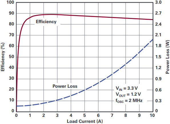
Figure 4. LTC3310S power loss vs. conversion efficiency.
Conclusion
Designing the optimum power conversion circuit for optical transport systems traditionally involves significant performance trade-offs in solution footprint, EMI performance, and power dissipation. Even seasoned switch-mode power supply designers will concede that maximizing all three is not possible. This is no longer the case. Analog Devices’ Power by Linear™ LTC3310S makes it possible to achieve small size, low EMI, and low power dissipation in a single IC power supply. This is particularly important in fiber optic communications equipment, where low EMI emissions are required to prevent data transmission from being compromised, and space is highly constrained.
About the Authors
Related to this Article
Products
Product Categories
{{modalTitle}}
{{modalDescription}}
{{dropdownTitle}}
- {{defaultSelectedText}} {{#each projectNames}}
- {{name}} {{/each}} {{#if newProjectText}}
-
 {{newProjectText}}
{{/if}}
{{newProjectText}}
{{/if}}
{{newProjectTitle}}
{{projectNameErrorText}}
Latest Media 21


