Abstract
In this application note, an external programmable current limit circuit for MAX38902 Low Drop-Out Linear Regulator is proposed. Having a programmable current limit adds an additional layer of protection in designing for variable load current requirements. MAX38902 has a rated maximum load current specification of 500mA and an in-built typical current limit of 700mA. In applications delivering few 100s of mA or LDOs used as current limit protectors, having the flexibility of a programmable current limit enhances product reliability and expands design opportunities with the LDO. In this application note, a reference design has been tested and validated with the current limit set at ~170mA with ±15% tolerance.
Introduction
Current limit in a LDO establishes an upper threshold for the current delivered. In a low dropout linear regulator architecture, the input and output average currents, which are connected by a series pass-through transistor, are almost the same.
Why current limit? Any surge in the current demanded by the load and/or triggered by a load fault condition results in an additional input current draw. If the device is not over current limited then this additional current can result in unacceptable system performance like increased load ripple, output voltage going out of regulation and, if not limited, can lead to system failure as well. Hence, there is a need to limit the current against these conditions in the interest of safeguarding the associated electronics within and outside the LDO so that it gracefully handles the fault condition (like output short circuit) and auto-recovers when the fault is removed.
There are multiple ways in which the current limit can be implemented.
Current Limiting Architectures
The types of current limiting architectures are as follows:
- Brick-wall current limiting: Load Voltage drops to zero once the set current limit is reached. Output voltage will not be in regulation during current limit condition.
- Constant Current upon exceeding I-limit: Once the current limit threshold is reached/ exceeded, this architecture will continue to deliver the current limited value to the load. Further reduction in load resistance will result in the output voltage droop from its target value while the device continues to deliver the current limited value to the load. (as described in this app note)
- Foldback-based current limiting: Load current folds back on exceeding the set current limit threshold.
- Peak current-based current limiting: This is common in inductor-based switched mode power supply architectures and uncommon in LDOs.
Each of these architectures have their own set of advantages/disadvantages and the choice of one architecture over the other is dependent on the application need, cost, total solution size, and performance.
About the MAX38902—Low Noise, Low Dropout, 500mA LDO
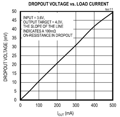
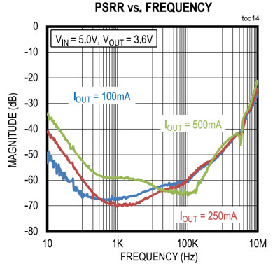
The MAX38902 are low-noise, linear regulators that deliver up to 500mA of output current with only 10.5µVRMS of output noise from 10Hz to 100kHz. These regulators maintain ±1% output accuracy over a wide input voltage range, requiring only 100mV of input-to-output headroom at full load. Figure 1 shows MAX38902 Dropout Voltage vs. Load Current. Figure 2 shows PSRR vs. Frequency. The key features and performance of MAX38902 LDO are listed in Table 1.
| Features | Performance |
Temp Range: -40C to 125C. Max TJ = 150C Available in two packages:
|
Figure 1. MAX38902 dropout voltage vs. output current.
Figure 2. MAX38902 PSRR vs. frequency. |
For the reference current limit design in this application note, consider the following operating conditions:
VIN = 4.0V, VOUT = 3.3V, Current Limit Set = ~170mA, ±15% tolerance
Programmable Current Limit Circuit Description
A MAX40009 push-pull, rail-to-rail input comparator is used to limit the current of the MAX38902 LDO. See schematic shown in Figure 3. A DC voltage rail of 4V powers up both the LDO and the comparator supply rails. A fixed reference voltage at noninverting comparator input is formed by the resistor-divider circuit R26 and R27 with its midpoint node tied to noninverting terminal of the comparator. The chosen resistor values of R26 and R27, as shown in Figure 3, set the reference voltage to 3.85V for a 4V input. A series 1? resistor senses the voltage drop proportional to the LDO current drawn. Following the resistor, the dropout voltage is fed to the inverting terminal of the comparator. Since the LDO current draw is proportional to the voltage drop across R25 and as the comparator inverting input voltage falls below 3.85V, the comparator output starts to switch high and limits the feedback voltage (FB) of LDO, thereby limiting the current.
Thus, increasing the resistance R27 reduces the current limit at constant input supply voltage and a single resistor can provide the control to have a programmable current limit.
In this example circuit, the current limit is set to ~170mA, ±15% based on tolerance stack up of resistors and comparator internal voltage transition threshold accuracy, Input Voltage DC variation/loading. For tighter tolerance, it is encouraged to use 1% tolerance resistors.
Design Considerations
- Current limit is applicable only for the chosen DC input voltage. If DC input rail changes, the Comparator reference voltage at the noninverting terminal changes, thus changing the current limit trip threshold. This can be overcome if a fixed zener voltage reference is used in place of R27. However, care should be taken in choosing the Zener voltage specification.
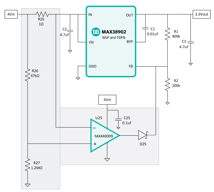
Figure 3. Schematic-added circuit block in gray. (R27 can be replaced by fixed zener with 1% or better tolerance).
- Resistance tolerances of R25, R26, and R27 all have a cumulative effect on the current limit trip threshold.
- The comparator rail-to-rail input allows for enough headroom for the comparator operation.
- What is rail to rail? Rail to rail means the signal under observation (input or output) can swing all the way to supply voltage level provided—either positive or negative rail voltage.
- Why rail-to-rail input is needed? The comparator input differential that determines the comparator output toggle is of the order of 15mV–20mV. If a voltage divider is used at the comparator inverting input terminal, this transition voltage resolution further reduces as this differential potential further gets divided among the resistors.
- Also post-R25, the resistor drop voltage is fed directly to the comparator negative terminal. There are two reasons for doing this.
- This avoids the sharing of drop voltage across an additional resistor divider thereby minimizing the comparator differential voltage input window for comparator output toggling.
- This means that voltage seen by comparator is few 100s of mV less than the input DC voltage supplied. Hence, the rail-to-rail input is needed.
- Op-amp vs. Comparator—things to look out for in this application note, the MAX40009 comparator is used. An op-amp can also be used, however, the following things need to be considered:
- Op-amp switching speed slew should be at least 150V/µS or higher. This is needed for the output of op-amp to switch quickly in the event of current limiting. Slower slew rate op-amps lead to unsatisfactory results.
- Op-amp common mode voltage across temperature should be as close to rail-to-rail, if not, at least have sufficient common mode headroom for input voltages used in the application.
- The op-amp/comparator chosen should have either the same or maximum overlap of supply voltage range as the LDO supply VIN range to avoid multiple input voltage rails powering up the system.
- The input supply voltage variation and circuit loading affect the reference voltage at the comparator noninverting input.
- Diode chosen at the output of comparator should be a fast recovery diode as speed of circuit operation in fault condition is critical. Schottky can also be chosen due to high switching speed, absence of reverse recovery time and lesser diode forward drop. However, the reverse current should be less—few µAs. In this application note, a Schottky diode of 30V, 0.37mV drop @100mA, 1.4µA leakage at VR = 10V is chosen, although the application just sees 0.6V reverse voltage under normal operation. Even if 500mA rectified current is not needed for average diode current, it is common knowledge that higher rectified current part has lesser diode voltage drop. A fast recovery diode can also be chosen considering the above guidelines.
Circuit Analysis in the Lab
The circuit behavior is explained with multiple waveforms for each operating corner.
Figure 4 shows the circuit operating in normal operation without any current limit where Figure 4(a) on the left shows the comparator input and output signal performance with LDO load current.
Channel 1: Iload,
Channel 2: Comparator noninverting input voltage (Vref),
Channel 3: Comparator inverting input voltage (post-R25 resistor drop Vsense),
Channel 4: Comparator Output Voltage
Figure 4a waveform is missing LDO Output voltage due to 4-channel scope limitation and hence 4b scope shot on the right in which Channel 2 is swapped for LDO 3.3V rail, the rest of the channel information remains the same as 4a. waveform is missing LDO Output voltage due to 4-channel scope limitation and hence 4b scope shot on the right in which Channel 2 is swapped for LDO 3.3V rail, the rest of the channel information remains the same as 4a.
Note that Figure 4 waveform collectively depicts steady state operation in which the comparator circuit does not limit the LDO output current, i.e., not in current limit.
All waveforms are annotated next to their measurements. Consider zooming-in on the waveforms to see this clarity.
Unless otherwise stated, the test conditions for waveform captured at 25C remain as follows VIN = 4.0Vdc, VOUT = 3.3V, Current Limit Set = ~170mA, ±15% tolerance
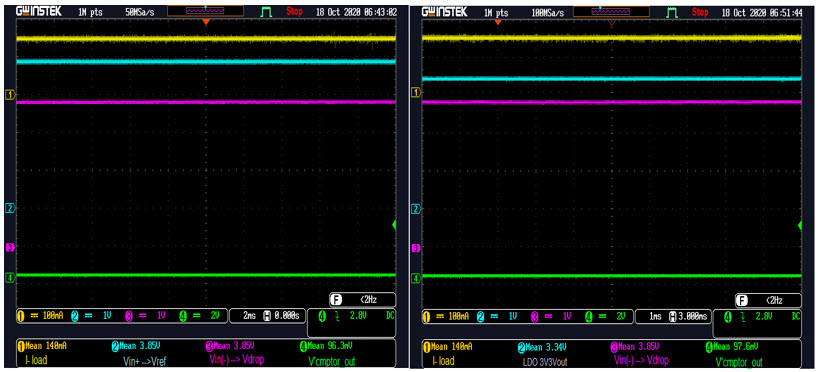
Figure 4. Normal operation—not in current-limit mode—4a-on-left, 4b-on right.
The next waveform capture in Figure 5 collectively depicts the steady state operation in which the comparator-based current limit circuit kicks in and limits the current to 165mA. The operating conditions remain the same as explained earlier. Observe that the voltage toggling of the comparator output on Channel 4 and 3.3Vout on Channel 2 in waveform 5b droops from 3.3V to 1.70V while in current limit.
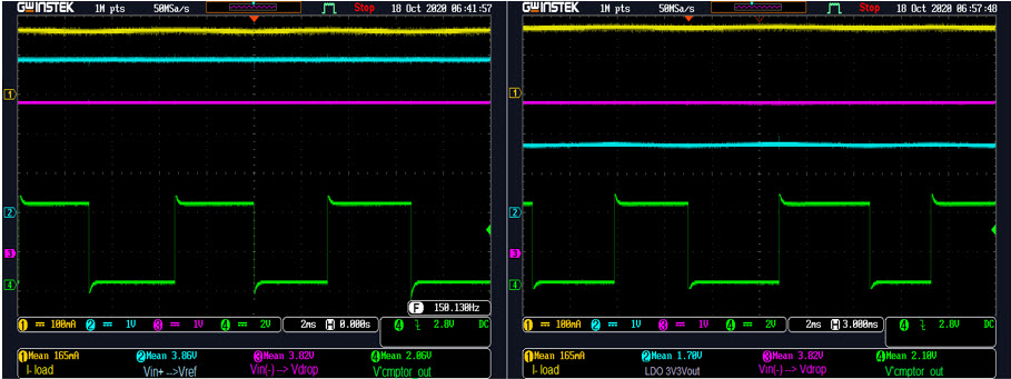
Figure 5. Steady state-current limit operation (Vin = 4Vdc, I-limit = 165mA). 5a- waveform on left, 5b- on right.
Next, in Figure 6, a single waveform shows a dynamic plot of circuit entering and exiting current limit accomplished with load resistance drop.
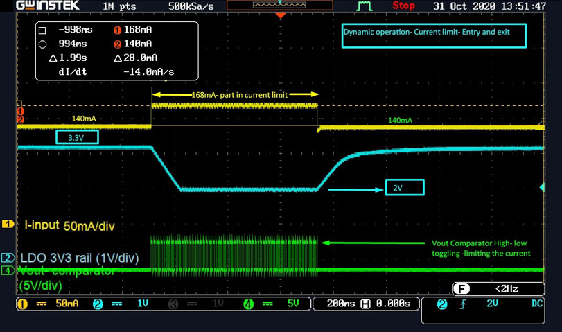
Figure 6. Dynamic current limit operation—entry & exit—load resistance drops from 24O to 14O.
Figure 7 depicts a sudden short circuit on load side while operating in normal operation delivering 3.3V output voltage and current of 140mA. As soon as short circuit is applied, observe that the LDO 3.3V rail drops to 0V on Channel 2. The peak input current seen by system during this condition is 240mA shown on Channel 1. Channel 4 shows that as soon as load short happens the comparator output voltage starts toggling from low to high, indicating that the system immediately enters current limit and after the peak current excursion of 240mApeak, settles to 160mA DC current limit for a persisting output short-circuit condition (observe Channel 1). The peak current seen is dependent on MAX38902 LDO bandwidth and limited by parasitics (trace inductances, cable inductances used in the circuit).
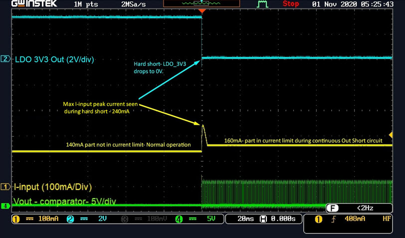
Figure 7. Hard short circuit during operating condition, current limit, and I-input peak.
Current Limit Behavior and Effect of Bypass Capacitance on Output Voltage Slew
The MAX38902 LDO uses a bypass capacitor (C1 in Figure 3) between OUT and BYP pin. This value ranges from 0.01µF to 0.1µF that sets the LDO output voltage slew during startup aiding in soft-start. Now, look at—LDO output voltage slew during the output short-circuit condition.
In this application schematic, C1, the bypass capacitance value chosen is 0.01µF, same as used in the MAX38902EVKIT#.
Startup Slew Rate = (5V/ms) × (0.01µF/CBYP)
where CBYP is in µF
(This formula flows from the LDO Architecture algorithm and is published in the MAX38902 data sheet in the Bypass (BYP) section under Detailed Description.)
Note that this slew rate applies only at startup. For recovery from a short-circuit per LDO internal bandwidth and architecture occurs at a slew rate approximately 500 times slower. (Refer to the MAX38902 data sheet Bypass (BYP) section under Detailed Description.)
In the waveform shown in Figure 8, a hard short is applied on load side during normal operating condition, however on release of short circuit, notice that the output voltage slew rate on short-circuit recovery is ~0.01V/ms for C1 = 0.01µF and the load current also gradually ramps up. This is an expected architecture behavior of soft-start after a short-circuit fault. Now, consider a case that asserts a load reset (different from a short circuit) and notice that Output Voltage slew rate is faster (as seen in the right portion of the waveform in Figure 8).
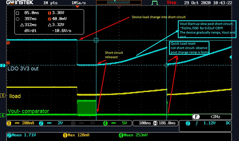
Figure 8. Soft-start LDO Vout slew influenced by bypass capacitor (C1 = 0.01µF).
The waveform in Figure 9 shows system startup in short-circuit condition.
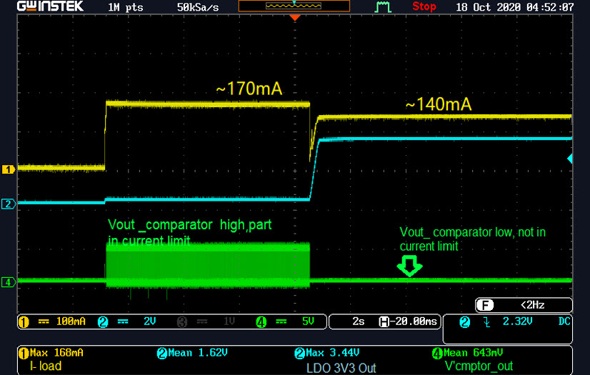
Figure 9. Startup with short circuit—current limit & recovery.
| Item | REF_DES | QTY | MFG PART# | Manufacturer | Description |
| 1 | R25 | 1 | CRCW06031R00FKEA | Vishay Dale | RES 1O, 1% 0.1W 0603 |
| 2 | R26 | 1 | RCA060347K0FKEA | Vishay Dale | RES 47kO 1% 0.1W 0603 |
| 3 | R27 | 1 | CRCW06031M20FKEA | Vishay Dale | RES 1.2MO 1% 0.1W 0603 |
| 4 | D25 | 1 |
NSR0530HT1G |
On Semi | Diode Schottky 30V 0.5A SOD323, 150C Tj |
| 5 | U25 | 1 | MAX40009 | Analog Devices | 220ns, Comparators with Shutdown, WLP. |
| 6 | C25 | 1 | CL05B104KO5NNN | Samsung Electronics | 0.1µF,16V,10%; X7R, 0402 |
Conclusion
In this application note, an external programmable current limit for LDO is designed and validated. The programmable current limit is needed in scenarios where system load short circuit, overcurrent scenarios due to incorrect load connections happen. In these scenarios, the fault current is limited by the impedance path taken by the current. Some applications such as lighter loads of few 100s of mA or LDOs used as current limit protectors require current limit to be configured to suit their end application. This provides an additional layer of protection and enhances system reliability. Through this application note, it is shown that by changing a single resistor R27, the current limit can be programmed to a desired value and the circuit can be reiterated for variable load current requirements across products. This flexibility greatly benefits designers, end consumers to quickly iterate the same circuit across their products, test, and reduce design to market time.
{{modalTitle}}
{{modalDescription}}
{{dropdownTitle}}
- {{defaultSelectedText}} {{#each projectNames}}
- {{name}} {{/each}} {{#if newProjectText}}
-
 {{newProjectText}}
{{/if}}
{{newProjectText}}
{{/if}}
{{newProjectTitle}}
{{projectNameErrorText}}
Latest Media 21


