Abstract
The DS26334 and DS26324 line interface units (LIUs) contain precise methods for making minor or major changes to the output pulse. This application note provides the information required to access factory test registers that allow the transmit waveform to be modified to meet a wide variety of application requirements.
With the addition of network-protection components and/or the need to route signals through connectors and other PCB requirements, it is sometimes necessary to manipulate the transmit waveform.
T1 and E1 Transmit Waveform Programmable Sections
The DS26334 and DS26324 contain registers that provide control for the transmit pulse in two major areas, amplitude and timing. T1 and E1 transmit pulses are divided into sections, each of which can be manipulated to provide the desired waveform. Figure 1 shows how the T1 pulse is divided and the registers that control each section. Figure 2 provides the same information for the E1 pulse.
T1 and E1 Transmit Waveform Amplitude Control
The amplitude of the DS26334 and DS26324 transmit pulse can be controlled in two ways.
- Adjusting the DAC gain
The LITXLAE register bits DAC[3:0] provide positive and negative adjustment of all the T1 or E1 levels simultaneously. - Partial waveform level adjustment
The WLA[3:0] bits of the level adjustment registers provide fine-tuning of specific sections of the waveform. The step size of the voltage level will change in proportion to the programmed DAC gain. If the DAC gain is increased by 10%, the step sizes will also increase by 10%.
T1 and E1 Transmit Waveform Timing Control
The timing of the DS26334 and DS26324 transmit pulse levels are controlled by the CEA[2:0] bits of the level adjustment registers. Each edge can be moved in both positive and negative directions in increments of 1/32 of TCLK.
General Recommendations
Modifying the DAC gain is the easiest method of controlling the amplitude of the transmit pulse because it will control the entire waveform with only one register change. Using the DAC gain first will allow for minimal (if any) modifications of the individual level adjustment registers.
The maximum output of the DAC will be affected by VDD. At lower levels of VDD, the maximum DAC gain setting might be unattainable. Changing VDD will also affect the maximum voltage attainable by the line driver's output stage.
Negative values do not use signed integer representation. The MSB is the sign bit and the LSBs represent magnitude, irrespective of sign. For example, a -3 in a WLA[3:0] register would be 1011b (bit 3 set to 1 means negative, 011 in the next three bits is magnitude 3) not 1101b (4-bit signed integer representation).
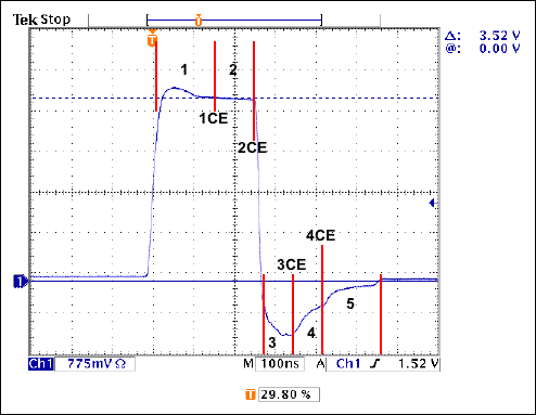
Figure 1. T1 pulse control sections.
T1 Pulse Control Sections
- Overshoot (1)
Register LTXLAA WLA[4:0] - Clock Edge (1CE)
Register LTXLAA CEA[2:0]
(1CE) = Clock edge transition from overshoot to plateau - Plateau (2)
Register LTXLAB WLA[4:0] - Clock Edge (2CE)
Register LTXLAB CEA[2:0]
(2CE) = Clock edge transition from plateau to falling edge - Undershoot (3)
Register LITXLAC WLA[4:0] - Clock Edge (3CE)
Register LITXLAC CEA[2:0]
(3CE) = Clock edge transition from falling edge to end of undershoot (3) - Undershoot (4)
Register LITXLAD WLA[4:0] - Clock Edge (4CE)
Register LITXLAD CEA[2:0]
(4CE) = Clock edge transition from end of undershoot (3) to end of undershoot (4) - Undershoot (5)
Register LITXLAC WLA[4:0]

Figure 2. E1 pulse control sections.
E1 Pulse Control Sections
- Overshoot (1)
Register LTXLAA WLA[4:0] - Clock Edge (1CE)
Register LTXLAA CEA[2:0]
(1CE) = Clock edge transition from overshoot to plateau - Plateau (2)
Register LTXLAB WLA[4:0] - Clock Edge (2CE)
Register LTXLAB CEA[2:0]
(2CE) = Clock edge transition from plateau to falling edge
Note: Registers LITXAC, LITXAD, and LITXAE are not used in E1 mode.
LIU Test Register Descriptions
Register Name: ADDP
Register Description: Address pointer
Register Address: 1Fh, 3Fh
| Bit # | 7 | 6 | 5 | 4 | 3 | 2 | 1 | 0 |
| Name | ADDP7 | ADDP6 | ADDP5 | ADDP4 | ADDP3 | ADDP2 | ADDP1 | ADDP0 |
| Default | 0 | 0 | 0 | 0 | 0 | 0 | 0 | 0 |
Bit 7 to 0: Address pointer (ADDP). This pointer is used to switch between pointing to the primary registers, the secondary registers, individual registers, BERT registers, and all the test registers. (See Table 1 for bank selection and Table 2 for the LIU test bank registers.)
| ADDP @ 1Fh ADDP7 to ADDP0 (Hex) |
LIU 1-8 Bank Name |
| 00 | Primary bank |
| AA | Secondary bank |
| 01 | Individual LIU bank |
| 02 | BERT bank |
| 03 | Reserved |
| 04 | LIU1 test bank |
| 05 | LIU2 test bank |
| 06 | LIU3 test bank |
| 07 | LIU4 test bank |
| 08 | LIU5 test bank |
| 09 | LIU6 test bank |
| 0A | LIU7 test bank |
| 0B | LIU8 test bank |
| ADDP @ 3Fh ADDP7 to ADDP0 (Hex) |
LIU 9-16 Bank Name |
| 00 | Primary bank |
| AA | Secondary bank |
| 01 | Individual LIU bank |
| 02 | BERT bank |
| 03 | Reserved |
| 04 | LIU9 test bank |
| 05 | LIU10 test bank |
| 06 | LIU11 test bank |
| 07 | LIU12 test bank |
| 08 | LIU13 test bank |
| 09 | LIU14 test bank |
| 0A | LIU15 test bank |
| 0B | LIU16 test bank |
| Addr | Abbr | Description |
| 00 | L1TXLAA | LIU 1 Tx level adjust A (test register) |
| 01 | L1TXLAB | LIU 1 Tx level adjust B (test register) |
| 02 | L1TXLAC | LIU 1 Tx level adjust C (test register) |
| 03 | L1TXLAD | LIU 1 Tx level adjust D (test register) |
| 04 | L1TXLAE | LIU 1 Tx level adjust E (test register) |
Detailed LIU Test Register Documentation
There is one bank of these registers for each LIU.
Register Name: LTXLAA
Register Description: LIU Tx level adjust A (overshoot voltage)
Register Address: 00H
Read/Write Function R/W
| Bit # | 7 | 6 | 5 | 4 | 3 | 2 | 1 | 0 |
| Name | WLA4 | WLA3 | WLA2 | WLA1 | WLA0 | CEA2 | CEA1 | CEA0 |
| Default | 0 | 0 | 0 | 0 | 0 | 0 | 0 | 0 |
Bits 7 to 3 : Transmit waveform levels adjust for output level 1 (WLA[4:0]). Moves magnitude from default ±360mV.
Bit 7 = sign bit ("1" means negative)
Bits 6 to 3 = magnitude (unsigned)
i.e, 24mV is LSB step size
Bits 2 to 0 : Clock edge adjust (CEA[2:0]). Moves clock edge ±3 32x-clks from default
<2> = sign bit ("1" means negative)
<1:0> = number of 32x-clks to move (unsigned)
Register Name: LTXLAB
Register Description: LIU Tx level adjust B (plateau voltage)
Register Address: 01H
Read/Write Function R/W
| Bit # | 7 | 6 | 5 | 4 | 3 | 2 | 1 | 0 |
| Name | WLA4 | WLA3 | WLA2 | WLA1 | WLA0 | CEA2 | CEA1 | CEA0 |
| Default | 0 | 0 | 0 | 0 | 0 | 0 | 0 | 0 |
Bits 7 to 3 : Transmit waveform levels adjust for output level 2 (WLA[4:0]). Moves magnitude from default ±360mV
Bit 7 = sign bit ("1" means negative)
Bits 6 to 3 = magnitude (unsigned)
i.e, 24mV is LSB step size
Bits 2 to 0 : Clock Edge Adjust (CEA[2:0]). Moves clock edge ±3 32x-clks from default
<2> = sign bit ("1" means negative)
<1:0> = number of 32x-clks to move (unsigned)
Register Name: LITXLAC
Register Description: LIU Tx level adjust C (undershoot voltage #1)
Register Address: 02H
Read/Write Function R/W
| Bit # | 7 | 6 | 5 | 4 | 3 | 2 | 1 | 0 |
| Name | WLA4 | WLA3 | WLA2 | WLA1 | WLA0 | CEA2 | CEA1 | CEA0 |
| Default | 0 | 0 | 0 | 0 | 0 | 0 | 0 | 0 |
Bits 7 to 3 : Transmit waveform levels adjust for output level 3 (WLA[4:0]). Moves magnitude from default ±360mV
Bit 7 = sign bit ("1" means negative)
Bits 6 to 3 = magnitude (unsigned)
i.e, 24mV is LSB step size
Bits 2 to 0 : Clock edge adjust (CEA[2:0]). Moves clock edge ±3 32x-clks from default
<2> = sign bit ("1" means negative)
<1:0> = number of 32x-clks to move (unsigned)
Register Name: LITXLAD
Register Description: LIU Tx level adjust D (undershoot voltage #2)
Register Address: 03H
Read/Write Function R/W
| Bit # | 7 | 6 | 5 | 4 | 3 | 2 | 1 | 0 |
| Name | WLA4 | WLA3 | WLA2 | WLA1 | WLA0 | CEA2 | CEA1 | CEA0 |
| Default | 0 | 0 | 0 | 0 | 0 | 0 | 0 | 0 |
Bits 7 to 3 : Transmit waveform levels adjust for output level 4 (WLA[4:0]). Moves magnitude from default ±360mV
Bit 7 = sign bit ("1" means negative)
Bits 6 to 3 = magnitude (unsigned)
i.e, 24mV is LSB step size
Bits 2 to 0 : Clock edge adjust (CEA[2:0]). Moves clock edge ±3 32x-clks from default
<2> = sign bit ("1" means negative)
<1:0> = number of 32x-clks to move (unsigned)
Register Name: LITXLAE
Register Description: LIU Tx level adjust E (undershoot voltage #3)
Register Address: 04H
Read/Write Function R/W
| Bit # | 7 | 6 | 5 | 4 | 3 | 2 | 1 | 0 |
| Name | WLA4 | WLA3 | WLA2 | WLA1 | WLA0 | CEA2 | CEA1 | CEA0 |
| Default | 0 | 0 | 0 | 0 | 0 | 0 | 0 | 0 |
Bits 7 to 4 : Transmit waveform levels adjust for output level 5 (WLA[3:0]). Moves magnitude from default ±180mV
Bit 7 = sign bit ("1" means negative)
Bits 6 to 4 = magnitude (unsigned)
i.e, 24mV is LSB step size
Bits 3 to 0 : DAC gain adjust (DAC[3:0]).
The following settings change the gain of the DAC.
0000 – Nominal DAC gain (default)
0001 – DAC gain +2.6%
0010 – DAC gain +5.3%
0011 – DAC gain +8%
0100 – DAC gain +11.1%
0101 – DAC gain +14.2%
0110 – DAC gain +17.7%
0111 – DAC gain +21.3%
1000 – DAC gain –2.2%
1001 – DAC gain –4.88%
1010 – DAC gain –7.11%
1011 – DAC gain –8.88%
1100 – DAC gain –11.11%
1101 – DAC gain –12%
1110 – DAC gain –15.1%
1111 – DAC gain –16.4%
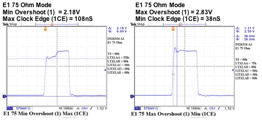
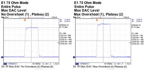
T1 and E1 Transmit Waveform Data
The following data was taken using the DS26324DK and is representative of the expected results for both the DS26334 and DS26324. The data is provided as a guideline for determining the range and method of using the level adjustment registers for controlling the amplitude and timing of the T1 and E1 transmit pulses. The data was taken at room temperature with a 3.3V VDD.

Figure 3. T1 normal operation.


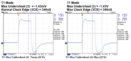


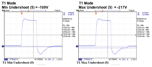
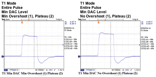


Figure 4. E1 120Ω normal operation.

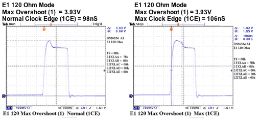


Figure 5. E1 75Ω normal operation.


DS26334 and DS26324 Information
For more information about our products, please consult the data sheets available on our website at T/E Carrier and Packetized Products.
If you have further questions concerning the operation of Analog devices, please contact the Telecommunication Applications support team.