Designing Single-Switch, Resonant-Reset, Forward Converters
Abstract
Among power-converter topologies, the single-transistor, forward converter is one of the most common for power levels below 100 watts. This article describes an improvement to that circuit called the \"single-transistor, resonant-reset, forward converter,\" which eliminates the reset winding and a diode (DTR). Several other advantages of this design will be discussed.
A similar article appeared in the October 2005 issue of Power Electronics Technology.
Introduction
Single-transistor, resonant-reset forward converters are commonly used in DC-DC converter modules for power levels below 100 watts. These devices are also quite useful for DC-DC converters with widely adjustable output voltages. This article, however, describes an improved circuit called the "single-transistor resonant-reset forward converter." This design eliminates the reset winding and a diode (DTR), and offers several distinct advantages.
The duty cycle for this resonant-reset converter can exceed 50%, making it suitable for low-cost DC-DC converters that operate from wide input voltages and deliver widely varying outputs. The absence of a reset winding reduces costs by simplifying the transformer, especially for the planar transformers widely used in high-density DC-DC converter modules. Finally, the resonant-reset circuit's sinusoidal reset voltage reduces EMI.
Conventional Single-Switch Forward Converter Design
To properly appreciate the resonant-reset topology, we must first understand the conventional single-switch forward converter (Figure 1a). When switch Q1 turns on, the transformer current rises from zero and the diode, DTR, is reverse biased. Transformer magnetizing current builds up to a value IM = VINTON/LM, where TON is the ON time per switching cycle and LM is the magnetizing current.

Figure 1a. Conventional single-transistor forward converter.
During the switch ON period, the load current, IO, is reflected in the primary as IP = IONS/NP, where NS is the number of secondary turns and NP is the number of primary turns. Output voltage is VO = VINDNS/NP, where D = TON/TS and 1/TS is the switching frequency. Magnetizing current in the transformer primary just before turn-off is VINTON/LM. When Q1 turns off, the transformer voltage tends to reverse. Voltage on the DTR cathode keeps increasing until DTR turns on.
For typical applications the NP/NR turns ratio is 1, where NR is the number of turns in the primary reset winding. The transformer magnetizing current now decreases from IM to zero. When it reaches zero, the transformer is fully reset and voltage across the transformer remains at zero until the next switching cycle starts. The maximum duty cycle, DMAX, in these applications is limited to 50%.
Resonant-Reset Forward Converter Design
Single-switch resonant-reset forward converters are characterized by the absence of a reset winding (Figure 1b). During the OFF time, the transformer resets (without loss) through a resonant circuit that consists of: the magnetizing inductance; and the combined capacitance of the switch, primary winding, and all reflected secondary capacitances including the rectifying-diode capacitance.
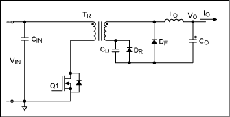
Figure 1b. Single-switch, resonant-reset forward converter.
Description of Operation
The following assumptions are made for this circuit analysis:
- The circuit has reached steady-state operation.
- LO and CO (fairly large) can be considered infinite.
- Leakage inductance is neglected.
- Drops due to the diode and switch on-resistance are neglected.
Steady-state operation for the circuit comprises three intervals in each switching cycle:
Interval 1
Initially, t = 0 and Q1 is ON (Figure 2a). The transformer is magnetized with a ramp current during the switch ON period. Secondary current flows through the secondary diode, DR, and the voltage across capacitance, CD, is approximately zero. CD includes the internal diode capacitance and the external capacitance added across DR. The primary magnetizing current has a value I1 at the start of this interval, and I2 at the end of the interval.
Primary current is the sum of the reflected current, IO(NS/NP), and the primary magnetizing current.
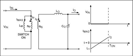
Figure 2a. From Figure 1b, an equivalent circuit for the voltage on Q1 and the primary magnetizing-current waveform during Interval 1 (not to scale).
Interval 2
When the switch is turned off, the switch drain-to-source voltage begins to rise (Figure 2b). When that voltage exceeds VIN, the secondary diode, DR, turns off and the freewheeling diode, DF, turns on. A sinusoidal demagnetization current starts to flow through the resonant circuit that is formed by the parallel combination of transformer magnetizing inductance, LM, and the capacitance, CR, reflected across the transformer primary. That capacitance, CR, is the sum of all capacitances across the primary, including the reflected diode capacitance, CD:

where CS is the primary switch capacitance and CT is the transformer primary capacitance. CD is the external capacitance across diode CD (diode capacitances << CD). Interval 2 ends at the end of TON + TR, where TR is one half of a resonant interval.


The external capacitance, CR, charges from zero to a peak value of  during this interval, and then discharges back to zero. The magnetizing current, I1, at the end of the interval should therefore equal -I2. Voltage on the primary switch at the end of this interval is VIN, but voltage on the switch reaches a peak of
  halfway through the interval.

Figure 2b. From Figure 1b, an equivalent circuit for the voltage on Q1 and the primary magnetizing-current waveform during Interval 2 (not to scale).
Interval 3
During this interval the diodes DR and DF are both ON; the primary switch is OFF (Figure 2c). Voltage across the transformer is zero, and the magnetizing current at the end of the interval equals -I2. This ends a switching cycle. Because the circuit is at steady state, the current I1 therefore equals -I2. Substituting for I1 in equation 1, we see that the primary magnetizing current at the start of each switching cycle is:

 . In that case a full half-cycle of resonance has not been completed before the next switching cycle begins. Therefore the voltage across the primary switch exceeds VIN at the start of each switching cycle. That condition increases the switching loss.
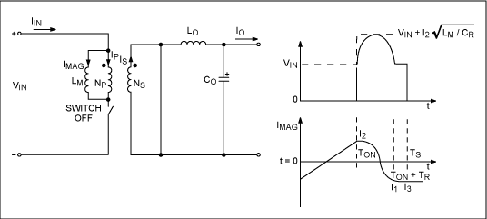
Figure 2c. From Figure 1b, an equivalent circuit for the voltage on Q1 and the primary magnetizing-current waveform during Interval 3 (not to scale).
Transient Operation
Transient stresses on the primary switch and secondary output diodes can vary greatly, depending on the type of controller used in the application. If the design is not optimal, transients can cause failure in the primary switches or the secondary diodes.
Consider operation with a current-mode PWM controller. Initially, the power supply operates at no load and high line voltage. A load transient is applied (minimum load to full load), which causes an immediate duty-cycle step to maximum duty cycle. In turn, that event causes a large increase in the transformer's magnetizing current, and may saturate the transformer unless its design accounted for such transients. The resonant-reset voltage is much higher than that during steady-state operation, and can cause failure in the forward diode or the primary switch.
To combat this problem, we introduce a volt-microsec clamp. Consider the controller above with a maximum-duty-cycle clamp that is inversely proportional to the input voltage. That arrangement limits the maximum flux excursion along the transformer's BH loop during a transient, which in turn allows the use of a smaller transformer. Transient-voltage stress on the forward diode and the primary switch is significantly less, but is still higher than during steady-state operation.
Now consider the operation of this converter type with a very light load, and using diodes for rectification. Magnetizing current is very close to zero during this mode of operation, and the duty cycle is low. If we now apply a load transient (from no load to full load), the duty cycle immediately increases to the maximum value allowed by the adaptive duty-cycle clamp. Before application of the transient, the magnetizing current is zero. The transient peak duty cycle at high line voltage is  , where VINMIN is the low-line input voltage, DMAX(TR) is the maximum duty cycle at low line voltage set by the adaptive duty-cycle clamp, and VINMIN is the input voltage at high line voltage. When a transient occurs, the magnetizing current increases from 0 to
  in the first switch ON cycle after the transient. Here LM is the primary magnetizing inductance and ƒSW is the switching frequency. After the switch turns off, the magnetizing current reverses in a sinusoidal fashion set by the magnetizing inductance, LM, and capacitance, CR. Peak voltage on the switch is:

For steady-state operation at full load and high line voltage, the peak steady-state voltage on the switch is:

where DMAX(S) is the steady-state duty cycle at full load and low line. In practical applications we try to set DMAX(TR) slightly higher than DMAX(S). We also see that the peak transient reverse voltage on the diode DF is more than twice as high as the peak steady-state reverse voltage with this type of PWM controller. For PWM controllers without the volt-microsec clamp, the transient voltage can be even higher.
If the circuit includes synchronous rectifiers, the inductor current does not become discontinuous and the magnetizing currents at light load and at full load are almost the same. For PWM current-mode controllers with volt-microsec clamps, the transient-voltage stress on the primary switch and the secondary diode, DF, is closer to the peak steady-state voltage stress.
The behavior of voltage-mode controllers is similar to that of current-mode PWM controllers. Again, the use of an adaptive volt-microsec clamp can reduce stress. These converter types often include a duty-cycle soft-start that ramps up the duty cycle, thus controlling any buildup of magnetizing energy while alleviating voltage stress.
Design Example
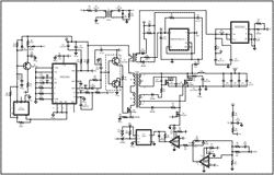
The working power supply of Figure 3 accepts DC input voltages in the range 36V to 56V, and produces a 4V to 18V isolated variable output voltage, controlled by an adjustable external reference. The maximum output current is 0.4A and the switching frequency, ƒSW, is 500kHz.
 OUT (36V to 56V) and output range 4V to 18V." class="img-responsive">
Figure 3. Resonant-reset forward converter with an input range of ground to -48VOUT (36V to 56V) and output range 4V to 18V.
The resonant-reset forward converter is most suitable for this design because it lets us maximize the duty cycle. That capability is necessary if the output voltage is to be properly controlled from high levels down to 4V. Otherwise, the PWM controller's minimum ON time is a limitation that can introduce problems. Synchronous rectifiers should be included to maximize efficiency and enable the PWM controller to control the output voltage down to 4V at light loads. The current-mode PWM controller shown also includes an adaptive volt-microsec clamp.
Adaptive Duty-Cycle Clamp
Because the power supply must turn on and provide full power at 36V, we set its turn-on point at 34.2V. That turn-on voltage includes a 5% margin to compensate for component tolerances. We then set the maximum duty cycle that corresponds to the turn-on point (set by the adaptive duty cycle) at 75%. That approach leaves 25% of the switching time available for resetting the transformer at the converter's lowest operating voltage.
Primary MOSFET Voltage Rating
At the lowest operating voltage, the maximum available reset time for the transformer is:
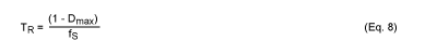
where DMAX = 0.75 and ƒSW = 5 x 10⁵. These values yield a reset time of 0.5µs. To minimize switching loss, the magnetizing current should complete one half-cycle of sinusoidal "resonant ringing" as given by Equation 4. Therefore,  , and the peak steady-state voltage stress on the primary switch (obtained by substituting values in equation 7) is 208.6V. Thus, for this design we choose a switch rated at 250V.
Transformer Design
Primary-to-secondary turns ratio for the transformer is n:
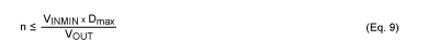
We choose a transformer with an EFD15 core of 3F3 material, and obtain n < 1.35 by substituting values in Equation 9. The actual primary turns (30) and secondary turns (24) yield a turns ratio of 1.25. The magnetizing inductance for this transformer, wound using ungapped cores, is 702µH ±25%. Tolerance in the magnetizing inductance could produce a tolerance of +11%/-13.4% in the transformer's self-resonant frequency, not accounting for tolerance in the total capacitance appearing across the primary in the actual circuit. The measured self-resonant frequency of a sample transformer was lower than 1MHz.
We must guarantee that the actual circuit's demagnetizing self-resonant frequency is higher than ƒSW/(1 - DMAX). We therefore gap the core, both to reduce the transformer's measured self-resonant frequency and to reduce the variation in magnetizing inductance. Using a gapped core with A1 tolerance of 10% yields an inductance of 144µH.
The self-resonant frequency measured for the new transformer sample is 4MHz; the transformer capacitance calculated from the expression for self-resonant frequency is 11pF. Based on the available reset time, the maximum allowable primary capacitance is 176pF. That latter value allows a maximum of 165pF for the sum of switch capacitance and reflected diode capacitance, CR. Because MOSFET capacitance is not easily determined, we must build the circuit and adjust the value of added capacitance across the synchronous MOSFET, QR, to get the appropriate reset time. In the actual power supply, the added capacitance across MOSFET QR is 100pF.
Output Inductor and Capacitor
The output inductor and capacitor are chosen to optimize efficiency and ensure compliance with the output-ripple specification. Thus, the inductor value is 47µH, and CO is formed by connecting three ceramic capacitors in parallel, each rated 4.7µF and 25V.
Primary MOSFET
For the primary MOSFET, Q1 (voltage rating of 250V), we choose an FQD4N25 from Fairchild for its low inherent capacitance and low on-resistance. This MOSFET also minimizes the gate-drive loss, conduction loss, and switching loss.
Synchronous-Rectifier MOSFETs
Peak stress on the synchronous rectifier, QR, is:

where na is the power transformer's actual primary-to-secondary turns ratio. In this case, na is 1.25 and the calculated value of VQR is 122V. We therefore choose a 150V MOSFET for QR. The peak voltage stress on the freewheeling MOSFET, QF, is:

where na is 1.25 and VINMAX is 56V. The calculated value is 44.8V, so for QF we choose a MOSFET rated at 60V. (The control circuit and synchronous MOSFET drives are shown in the schematic, but not discussed further.)
Experimental Results
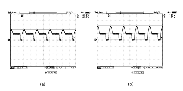
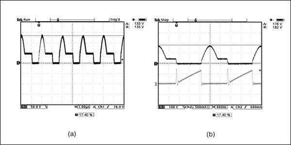
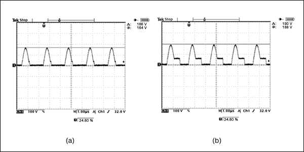
Figures 4, 5, and 6 show voltage waveforms on the primary MOSFET of Figure 3 at different input voltages and various output voltages, and with an output load of 400mA. The drain-voltage waveforms clearly show that the resonant-reset voltage does not vary with line voltage, but is proportional to the output voltage. Peak voltage on the primary MOSFET is equal to the input voltage plus the resonant-reset voltage.
 DS on Q14 at an input of 48VDC, with output voltage at 4V (a) and 8V (b)." class="img-responsive">
Figure 4. From Figure 3, VDS on Q14 at an input of 48VDC, with output voltage at 4V (a) and 8V (b).
 DS on Q14 at an input of 48VDC, with output voltage at 12V (a) and 18V (b)." class="img-responsive">
Figure 5. From Figure 3, VDS on Q14 at an input of 48VDC, with output voltage at 12V (a) and 18V (b).
 DS on Q14 at an input of 36VDC (a) and 56VDC (b)." class="img-responsive">
Figure 6. From Figure 3, output voltage at 18V, with VDS on Q14 at an input of 36VDC (a) and 56VDC (b).
Conclusion
Resonant-reset forward converters are quite suitable for power supplies operating from wide-range DC-voltage inputs. They are also suitable for applications requiring a wide range of adjustable output voltage. In designing resonant-reset forward converters, you should minimize the stress of transient voltages on the devices; using synchronous rectification reduces transient-voltage stress on the power semiconductors. For optimum performance you should also choose an appropriate controller.
Latest Media 21


