Current-Source DAC with PIN Diode Provides RF Attenuation and Thermal Compensation
Abstract
RF attenuation is a common circuit in wireless designs. This application note details several methods used to control RF attenuation using a PIN diode, as well as a current-source DAC.
PIN diodes are often used as variable attenuators for RF signals in TV tuners, and for wideband RF in fixed equipment. These diodes can be mounted as discrete devices on a board, or integrated into hybrid GaAs modules. At a high-RF frequency, the forward resistance of a PIN diode decreases with increasing DC current through the junction (Figure 1).
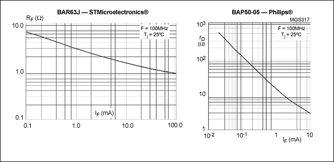
Figure 1. Resistance vs. forward current for a typical PIN diode.
PIN-diode attenuators can operate in a series or shunt configuration. A series attenuator (Figure 2a) typically requires 10mA to 20mA through the diode. Its attenuation is:
20log(1 + RPIN / 2Z0) (in dB)
For a shunt attenuator (Figure 2b), the required bias current is typically 2mA to 3mA. The attenuation for a shunt attenuator is:
20log(1 + Z0 / 2RPIN)(in dB)
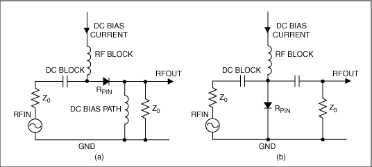
Figure 2. An RF signal can be attenuated by a series (a) or shunt (b) PIN diode.
A system controller adjusts the attenuation by varying current through the diode.
The system may also require temperature compensation (Figure 3). In this simplified circuit, a digital potentiometer IC (digipot) sets the fixed or adjustable bias level, and a thermistor provides the temperature input. These inputs are combined in an op-amp circuit, and the output is converted to current by driving the PIN diode through a resistor.
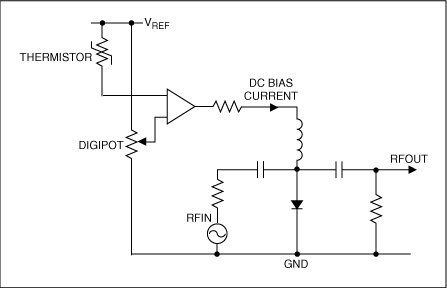
Figure 3. A simplified bias circuit for the PIN diode.
This implementation is not straightforward. The thermistor response must be matched to the PIN diode, and bias-current changes can alter the PIN diode's DC forward voltage, which in turn causes nonlinearity in the bias current. You could replace the thermistor and digipot with a voltage-output DAC and compensate the circuit digitally, but that approach would not eliminate the diode's forward voltage. A much better alternative is to introduce a current-source DAC (see the Appendix for ideal examples).
The Figure 4 circuit includes a hybrid quadrature-matched shunt attenuator and a pair of matched PIN diodes, which are driven by a single DAC output. Ambient temperature is measured by an analog or digital sensor connected to the host microcontroller, which uses a lookup table (LUT) or algorithm to implement the temperature compensation. The desired attenuation passes through the LUT or algorithm to give the PIN current needed, which is then set by the DAC. Current through the PIN-diode junction is set only by the DAC, and is independent of the diode's forward voltage or any other DC impedance in the connection.
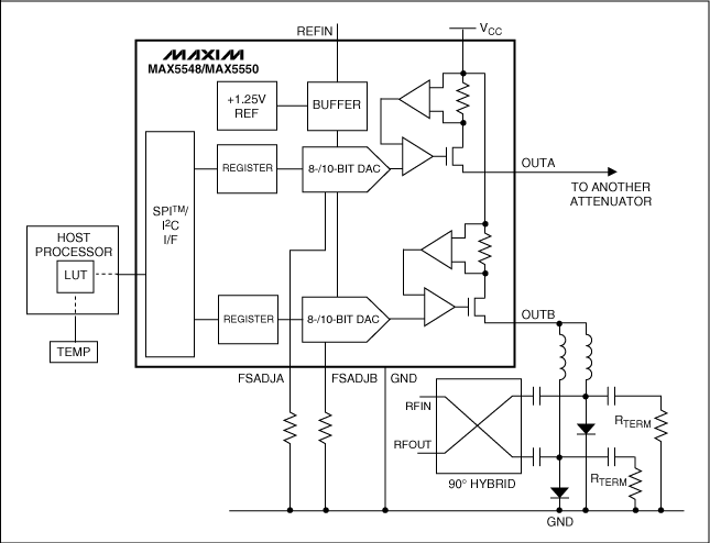
Figure 4. This RF attenuator is driven by a current-output DAC (MAX5548 or MAX5550), which compensates for temperature by adjusting its output current according to correction signals from the host processor.
Filter on Output
For circuits that include RF-blocking inductors and capacitors (to eliminate unwanted DC paths), the outputs remain stable with more than 100nH of series inductance and 10nF of capacitance to ground. As one benefit of a current (vs. voltage) output, series resistance introduced by the filter has no effect on accuracy, provided the resulting voltage drop remains within the DAC's range of output-compliance voltage.
Appendix—DAC Examples
The MAX5548/MAX5550 are dual 8-/10-bit DACs with current-source outputs and a compliance range of 4V at 30mA. Both outputs can source up to 30mA, and they can be paralleled for high-current applications up to 60mA. Operating from a single supply of +2.7V to +5.25V, these devices draw typical supply currents of 1.5mA per DAC in normal operation, and less than 1µA maximum in shutdown mode. Output-leakage current in shutdown mode is only ±1µA maximum.
To ensure high accuracy and low-noise performance, each IC includes a +1.25V bandgap reference and a control amplifier. They also offer the option of connecting an external reference (REFIN) for improved gain accuracy. The parts are compatible with the I2C and SPI serial interface, as selected by a pin on the package. In SPI mode, the parts can be daisy-chained to save processor I/O pins and, for an I2C interface, four pin-selectable addresses are available. Software and an external resistor for each output determine the maximum value for programmable output current.
A similar article appeared on Planet Analog.com on May 31, 2006.
Related to this Article
Products
PRODUCTION
Dual, 8-Bit, Programmable, 30mA High-Output-Current DAC
PRODUCTION
Dual, 10-Bit, Programmable, 30mA High-Output-Current DAC
Product Categories
{{modalTitle}}
{{modalDescription}}
{{dropdownTitle}}
- {{defaultSelectedText}} {{#each projectNames}}
- {{name}} {{/each}} {{#if newProjectText}}
-
 {{newProjectText}}
{{/if}}
{{newProjectText}}
{{/if}}
{{newProjectTitle}}
{{projectNameErrorText}}
Latest Media 21


