Abstract
A complete GPS solution is achieved with minimal external components, using the MAX2742 integrated CMOS RF front-end GPS receiver.
Introduction
The MAX2742 is a CMOS, single-chip, GPS front-end downconverter. This state-of-the-art device consumes very low power (32mW at 2.4V), and eliminates the need for a costly IF SAW filter or bulky discrete IF bandpass filters. The MAX2742 integrates a low-noise amplifier (LNA), mixer, BPF, automatic-gain-control amplifier (AGC), local oscillator synthesizer, clock buffer, and internal digital sampler.
This device can interface with many commercially available GPS baseband ICs. It is suitable for many applications, including vehicle navigation, telematics, automatic security, asset tracking, location-based service (LBS), and consumer electronics. The external components required around the device are minimal for a complete GPS RF solution. The system block diagram can be found in the following section.
The MAX2742 works with an 18.414MHz* crystal or TXCO, and offers differential or single-ended** IF output at 1.023MHz. Total signal conversion gain is 120dB, with a noise figure of 4.5dB. The IF signal is sampled at the reference clock rate of 18.414MHz.
For more details, please refer to the MAX2742 data sheet.
* Note: 18.414MHz is 18 times 1.023MHz, which is one-tenth of the GPS fundamental frequency 10.23MHz.
** Note: There are three IF output pins—one pair of differential outputs and one single-ended output. Selection is controlled by pin 10.
Complete GPS RF Front-End Solution
Figure 1 shows the important building blocks and features of Maxim's complete GPS RF solution. Description of the building blocks can be found in Table 1; cascaded performances are shown in Table 2. Figure 2 shows the application circuit of the GPS receiver RF portion with the MAX2742.
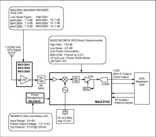
Figure 1. GPS RF front-end block diagram.
| Block | Description | Note |
| GPS antenna | Active GPS antenna, commonly has ~1.5dB NF and ~20dB gain | |
| LNA | MAX2641/MAX2654/MAX2655 LNA | External LNA is required when active GPS antenna may not be present. |
| RF SAW | RF bandpass filter centered at 1575.42MHz | RF BPF is required for jammer immunity |
| Power management | MAX8510 low-noise LDO | |
| RF downconverter | MAX2742 | |
| Reference clock | 18.414MHz crystal/TCXO | |
| DSP | Baseband processor |
| Specification | Cascaded Performance | Note |
| Gain | 131dB | Without active antenna, assuming 15dB external LNA gain, 3dB BPF loss, and 1dB matching network loss |
| Noise Figure | 1.9dB | Without active antenna, assuming 1.5dB external LNA NF. |
| Power Consumption | 20mA | MAX2744+MAX2654 as an example |
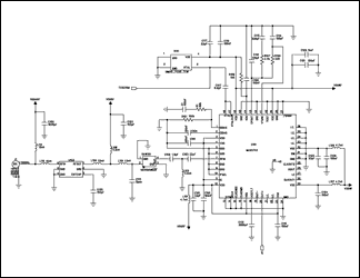
Figure 2. GPS RF portion schematic for MAX2742.
Complete Stand-Alone GPS Receiver Solution
There are more building blocks to construct a complete GPS receiver, other than just the RF plus baseband IC. As shown in Figure 3, an extra antenna supply-control block, a RESET circuit, and a delay circuit are needed. Description of the building blocks can be found in Table 3; cascaded performances are shown in Table 4.
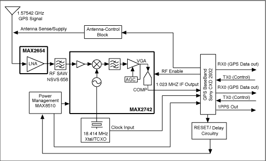
Figure 3. Complete GPS receiver solution block diagram.
| Block | Description | Note |
| GPS Antenna | GPS Antenna | Refer to the RF portion for details. |
| LNA | MAX2654 LNA | Refer to the RF portion for details. |
| RF SAW | RF bandpass | Refer to the RF portion for details. |
| Power management | MAX8510 low-noise LDO | |
| RF downconverter | MAX2742 | |
| Reference clock | 18.414MHz TCXO | The TCXO also supplies the baseband clock. In this reference design, GPS clock output from the MAX2742 is not used. |
| GPS baseband | Sony CXD2932 | The CXD2932 also controls active antenna supply, RESET function. See details below. |
| Antenna control block | Antenna supply control with p-MOSFET and current-sense resistor | The sense resistor feeds the antenna supply information back to CXD2932. There are three possible conditions: normal, short, and open. |
| RESET/delay circuitry | Different levels of RESET, and delay circuit required by CXD2932 | To ensure successful startup, CXD2932 requires two RESET signals 100ms apart. |
| Baseband interface | TX: external control command | |
| RX: GPS data out | Data-rate programmable | |
| 1PPS: one pulse-per-second signal | This signal is aligned with GPS atomic clock. |
Figure 4 shows the real PCB layout of the reference design. The complete solution only occupies 25mm x 25mm of PC board space.
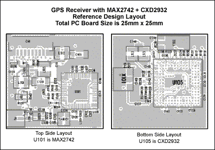
Figure 4. GPS Receiver PCB layout.
| Block | Description | Note | Block | Description | Note | Description | Note |
| 1 | Power supply | VCC | (Note 1) | 2.7 ~ 3.6 | T.C. | V | |
| 2 | Current consumption | ICC | VCC = 3.0V | 91 | 88 | mA | |
| 3.1 | Sensitivity | Sens | Acquisition | Tracking | -145 | -145 | dBm |
| 3.2 | -138 | -138 | |||||
| 4 | TTFF | TFC | Cold start | 58 (typ) | 60 (max) | s | |
| 5 | TFW | Warm start | 45 | 30 (max) | s | ||
| 6 | TFH | Hot start | 17 | 6 (max) | s | ||
| 7 | Position drift range | PR | 95% possibility | 100 | 90 | ft | |
| 8 | 1PPS output accuracy | 1PPS | 1 | N.M. | ns | ||
| Note 1: T.C. = test condition, N.M. = not measured. | |||||||
Related to this Article
Products
1575MHz/1900MHz Variable-IP3 Low-Noise Amplifiers
1575MHz/1900MHz Variable-IP3 Low-Noise Amplifiers
300MHz to 2500MHz SiGe Ultra-Low-Noise Amplifiers
Product Categories
Latest Media 21


