A BPSK Modulator for 2GHz to 12GHz
Binary phase-shift keying (BPSK), also known as bi-phase modulation, is a simple, popular digital modulation scheme. The symbol constellations are as far apart as possible, which is desirable for weak signal work. BPSK is also popular for its relatively simple spectrum-spreading capability. Thus BPSK finds applications in weak signal communications, spread-spectrum, ranging and radar systems[1].
The LTC5548 is fundamentally a passive double-balanced mixer with a DC-coupled IF port. As a BPSK modulator (Figure 1), the mixer provides no frequency translation, hence the modulator frequency range is limited to that which both the LO and RF ports can handle. Figure 2 shows the test setup for the BPSK modulator. A lab-grade vector signal generator with differential outputs generates the baseband waveforms.

Figure 1. RF mixer used as BPSK Modulator. Resistors R1 and R2 build up each of the IF inputs to be 50Ω, suitable for driving with modern lab test equipment.
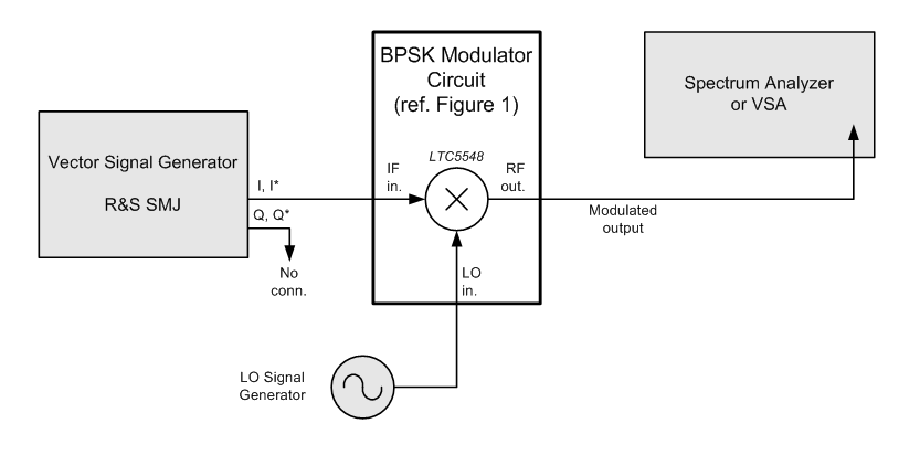
Figure 2. Test setup for the BPSK modulator.
Modulator IF Input Signals
Baseband drive level at the LTC5548 DC-coupled IF input should be in accordance with the following guidelines:
- Drive should always be differential (balanced), with 0.0V common-mode.
- Typical drive level at each IF pin can be ±0.1V continuous (0.2VP-P).
- Drive level at each IF pin should not exceed ±0.2V on the signal peaks (0.4VP-P).
Drive level at each IF pin must never exceed the ±0.3V absolute maximum rating. Furthermore, such large input signals generally produce unacceptably high spectral regrowth at the RF output.
For most applications, low LO leakage is required, which means DC offset voltage across the IF input pins should be near zero volts. Typically, the LO leakage is at a phase that cannot be completely cancelled with a DC offset trim. Consequently, LO leakage can be reduced but not eliminated using DC offset trim.
Figure 3 shows the IF+ and IF– pin voltages, which compose the differential IF input signal. The test circuit is as shown in Figure 1. Note the signal is differential and centered at approximately zero volts, and complies with the drive level criteria listed above.
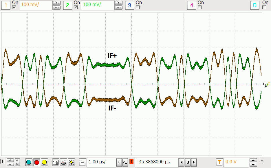
Figure 3. Typical modulator drive waveforms, measured at IF+ and IF- input pins. Symbol rate = data rate = 5Mbps.
Applications that radiate the BPSK signal over-the-air tend to benefit from digital filtering of the baseband source. In other applications, the modulated signal bandwidth may not be an issue, requiring little-to-no baseband filtering. Figure 4 illustrates the modulator output spectrum, both with and without baseband filtering.
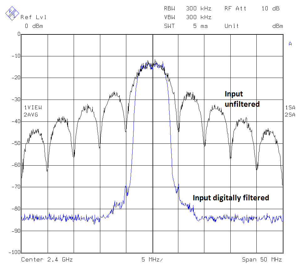
Figure 4. Modulator output while driven with 5Mbps PN9 data. Digital input filtering provides the pulse shaping that is highly effective at reducing output bandwidth. Here, the digital filter choice is a root-raised cosine response, alpha = 0.35. Trace averaging masks the 4.0dB peak-to-average ratio on the digitally filtered signal.
Example 1: 2.4GHz BPSK Modulator
A vector signal analyzer (VSA) measures the BPSK modulation accuracy of the LTC5548. The modulator schematic is as shown in Figure 1, and each differential input pin signal is driven as shown in Figure 3. The test setup is as shown in Figure 2. EVM measures better than 0.5% rms, satisfactory for a BPSK communication system.

Figure 5. BPSK modulation accuracy at 2.4GHz. The VSA measurement filter is a root-raised cosine response, alpha = 0.35. Output power measures –2.6dBm.
Example 2: 8.6GHz BPSK Modulator
With the same circuit tested at 8.6GHz, we see the output power reduced, and LO leakage increased. The increased phase error is attributable to increased phase noise of the LO at the higher frequency, and also higher residual phase noise of the VSA at the higher frequency. Overall modulation accuracy of EVM = 0.6% remains acceptable for BPSK.

Figure 6. Modulation accuracy at 8.6GHz. Output power measures –5.8dBm.
Example 3: 12 GHz BPSK Modulator Using the Internal ×2 LO Multiplier
In this test, we increase the LO frequency to 12 GHz, derived from the internal LTC5548 LO frequency doubler. In this manner, the test also includes any residual phase noise error that the LO doubler may contribute. External LO drive is 6GHz, and ×2 (pin 8) is tied high.
The VSA shows only a slight, gradual performance degradation, compared to lower frequencies. EVM is better than 0.8%, acceptable for BPSK applications.
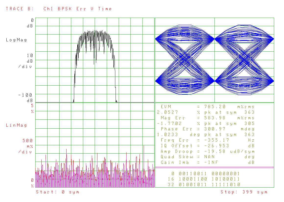
Figure 7. Modulation accuracy at 12GHz using internal LO ×2 multiplier. Output power measures –9 dBm at 12GHz.
Conclusion
The EVM measurements indicate that as LO frequency increases, EVM and LO leakage (IQ offset) gently degrade, but performance remains acceptable for BPSK applications.
In all three above examples, symbol rate = 5Msps. If operating at higher LO frequencies and wider bandwidths (faster symbol rates), EVM will increase due to the high-frequency roll-off of the modulator RF port. For these high symbol rate (or high chip rate) applications, designers should conduct their own measurements to confirm that modulation accuracy remains acceptable.
[1] For example, CDMA, GPS, WiMAX, WLAN, and ZigBee to name a few.
About The Authors
Related to this Article
Products
{{modalTitle}}
{{modalDescription}}
{{dropdownTitle}}
- {{defaultSelectedText}} {{#each projectNames}}
- {{name}} {{/each}} {{#if newProjectText}}
-
 {{newProjectText}}
{{/if}}
{{newProjectText}}
{{/if}}
{{newProjectTitle}}
{{projectNameErrorText}}
Latest Media 21


