Analyzing IC Heat Dissipation? Forget the Software Modeling, Use Your Pencil!
Abstract
When a component is performing a function, whether it’s frequency conversion, dc-to-dc conversion, or power amplification, if the efficiency is less than 100%, then some of the energy will be dissipated in the form of heat. This is referred to as dissipated power (PDISS). This article will discuss the calculations, layout, and performance trade-offs associated with PDISS. The major contributors to PDISS in a surface-mounted circuit are the component junction temperature, thermal resistance, PCB material, and via structures. With good modeling and layout technics, a clever system designer can minimize the effects of PDISS.
Despite significant advances made by electronic designers in developing products that perform complex tasks, system designers may encounter performance limiting factors beyond electronic circuitry—like thermal management. Even if good design practices and reliable components are in place, system performance can suffer if appropriate temperature controls are not implemented. That’s why circuit designers should have a basic understanding of how to model, manage, and implement temperature mitigation techniques.
Heat is transferred from high temperature objects to lower temperature objects by conduction, radiation, or convection.
Heat Sinks
The most widely used thermal management device, the heat sink, transfers heat by conduction from a semiconductor to a specially constructed metal plate. The most common heat sinks include dense metal with a large surface area (fins). The metal’s high thermal conductivity transfers the heat from the semiconductor to the heat sink, and then to the surrounding air. The heat sinks ability to transfer heat depends on its material, geometry, and overall surface heat transfer coefficient.
Semiconductor Material for RF Circuit Design
RF integrated circuits (ICs) or monolithic microwave integrated circuits (MMICs) use semiconductor material for designing electronic circuits. Final stage RF amplifiers and supporting dc supply components have very high power density needs, and therefore, generate significant heat. The main sources of this dissipated power (PDISS) is I2R loss. Various semiconductors have more or less power density capabilities. The graph in Figure 1 shows some of the more common semiconductors used in RF design, and their power density and maximum frequency ability.

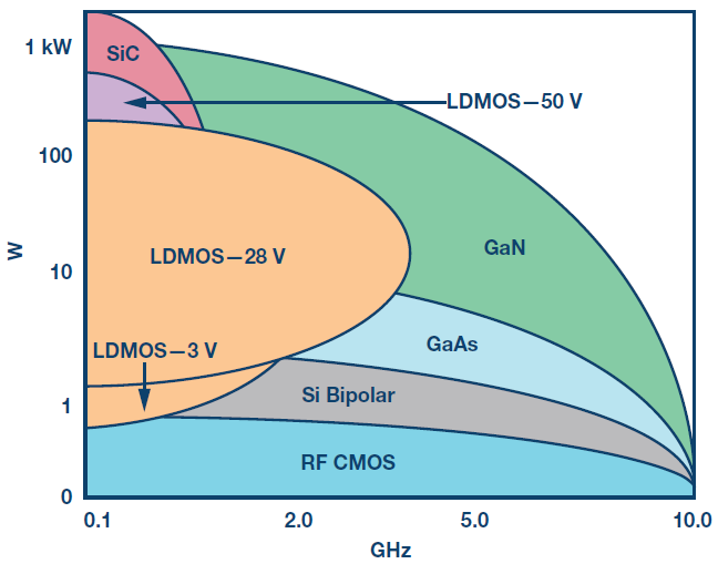
Figure 1. FET power and frequency vs. IC process.
GaN is Disruptive
Solid-state power amplifiers (SSPAs) are not a new technology. GaAs (gallium arsenide) and LDMOS (laterally diffused metal oxide semiconductors) have been used for high power amplifiers for many years. Silicon-based LDMOS FETs are widely used in RF power amplifiers for base stations, as the requirement is for high output power with a corresponding drain, to source breakdown voltage usually above 60 V. Compared to other devices, such as GaAs FETs, they show a lower maximum power gain frequency. LDMOS FETs operate with the highest efficiencies below 5 GHz. A gallium arsenide field effect transistor (GaAsFET) is a specialized type of FET that is used in solid-state amplifier circuits at microwave radio frequencies. This spans the spectrum from approximately 30 MHz up to the millimeter wave band.
The GaAs FET is known for its sensitivity and especially, for the fact that it generates very little internal noise. The power density is limited by the breakdown voltage—you can get 20 V breakdown on a good day with a GaAs MESFET. LDMOS allows for high power, but operates below 5 GHz. GaAs MESFETs operate at very high frequencies, but the low breakdown voltage limits them to the 10 W power range. Gallium nitride and silicon carbide (GaN on SiC) are both wideband gap material, which means the combined breakdown voltages are as high as 150 V. This allows higher power density, along with a lower load line for easier impedance matching. GaN on SiC allows power gain at frequencies in the millimeter bands (Ft~ = 90 GHz, FMAX ~200 GHz).
The performance of GaN on SiC is limited most by thermal transfer; getting the heat away for the device is the last issue to unravel. Previous generation RF power amplifiers were generally available in flange mount packaging that inherently provided a mechanical and thermal mount for these devices, directly to a metallic carrier. These mechanically mounted devices could not be surface-mounted on a circuit board and, as a result, increased the product cost. Current generation RF power amplifiers are generally available in surface-mount QFN packages that can be attached to traditional PCB’s, via mature reflow soldering processes. With careful planning and modeling, even GaN on SiC amplifiers can be surface mounted on PCBs.

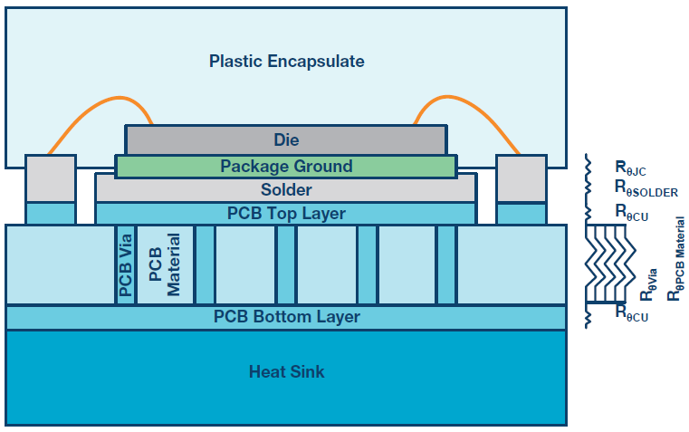
Figure 2. Cross section of surface mount QFN package attached to traditional PCB.
With this new package style, the PCB now has to function not only as the RF interconnection between devices, but also as the path to conduct heat away from the power amplifier. The ability of the PCB to conduct heat depends directly on the materials, layout, and design of the PCB. The following section will detail the methods needed to analyze the PCB design to ensure it will serve as an adequate thermal interface between the RF power amplifier and the heat sink.
All of the thermal management questions that arise from this discussion can be answered by carefully modeling the thermal performance of the component and the material of the PCB it’s attached to. The following is pretty straightforward algebra. The formulas can be entered into a spreadsheet to make it easier to calculate the thermal resistance.
Thermal Resistance
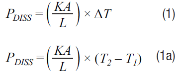
In order to model the thermal performance of the system, we can treat the thermal energy like an electrical system. The total dissipated power (PDISS) in watts is equal to the thermal conductivity coefficient (K), multiplied by the cross sectional area (A), perpendicular to direction of heat dissipation over the length (L) the heat will travel. The above is then multiplied by the change in temperature from the beginning of surface to the final surface (ΔT).
Where Rθ is the thermal resistance between surfaces.
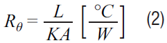
Substitute in thermal resistance.
From these equations we can calculate the maximum case temperature (TCMAX). This is the temperature of the surface of the packaged component. The case temperature will be the maximum junction temperature (TJMAX) given in the data sheet, minus the thermal resistance of all of the materials between the junction and the case (RθJtoC), given in the data sheet, multiplied by the internal dissipated power (PDISS). The internal dissipated power is the difference between all of the power put into the component (dc and RF), and the power that comes out of the component.

Equivalent Thermal Resistance
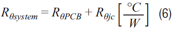
This is where you have to do your homework. Refer to Figure 1 to see all of the various thermal resistance you will need to calculate. RθCase to plate is the equivalent thermal resistance of all of the materials, between the package ground and the heat sink. To calculate the thermal resistance of the materials in your thermal circuit, you will need to know exactly what materials are in the heat path. Some likely candidates are: solder, ½ oz. Cu, and PCB material.
The thermal resistance of your stack up is not given, therefore, you will calculate the individual thermal resistance and add them, just as you would resistors in an electrical circuit.
Example: The typicall solder thickness under the component ground slug is 2 mils (0.002 in). A 3 mm (0.118) by 3 mm ground slug has the area of 9 mm2 or 0.014 in2 . The thermal conductivity of solder is 1.3 W/in-ºK.
From (2)

L is the thickness of the material
A is the area of the material
K is the thermal conductivity of the material

Some common thermal conductivity properties are listed in Table 1. Continue the calculations for all of the material in the heat path from the case to the heat sink. Add the resistance just as you would resistors in an electrical circuit.
| Material | Thermal Conductivity | |
| W/m-°K | W/in-°K | |
| Alumina | 18.0 | 0.5 |
| Alumina (AI203) | 27.6 | 0.7 |
| AuSn solder | 57.0 | 1.4 |
| Solder (Sn63) | 50.0 | 1.3 |
| Copper | 400.0 | 10.2 |
| Aluminum Nitride | 237.0 | 6.0 |
| Tungsten | 160.0 | 4.1 |
| Siver | 419.0 | 10.6 |
| Gold | 318.0 | 8.1 |
| GaN | 225.0 | 5.7 |
| Indium Phosphide (GaO) | 68.0 | 1.7 |
| Gallium Phosphide | 110.0 | 2.8 |
| Indium Nitride (InN) | 45.0 | 1.1 |
| GaAs | 59.1 | 1.5 |
| Sapphire | 40.0 | 3.3 to 5.7 |
| Silicon | 150.0 | 3.8 |
| Diamond | 1100.0 | 27.9 |
| Rogers 4350 (RO4350) | 0.6 | 0.0 |
| Thermal Conductive Epoxy | 0.8 | 0.0 |
| Plastic Mold Compound | 0.7 | 0.0 |
| Si | 130.0 | 3.3 |
| Ge | 58.0 | 1.5 |
| SiC 3C | 360.0 | 9.1 |
| SiC 4H | 370.0 | 9.4 |
| SiC 6H | 490.0 | 12.4 |
| AlAs | 0.0 | 0.0 |
| GaAs | 55.0 | 1.4 |
| InAs | 27.0 | 0.7 |
| SiGe | 110.2 | 2.8 |
| AlGaAs | 129.9 | 3.3 |
| InGaAs | 55.1 | 1.4 |
| InAlAs | 129.9 | 3.3 |
| InAsP | 129.9 | 3.3 |
| GaAsP | 55.1 | 1.4 |
| InGaP | 55.1 | 1.4 |
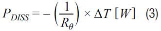
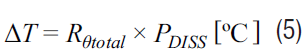
Now we know the total dissapated power form Equation 4 and the total equivalent thermal resistance from the calculations above using, Equation 2. When we rearrange Equation 3, we can see that the rise in temperature is equal to the product of the dissipated power and the total equivalent thermal resistance.
This is important because now we can calculate the temperature rise from the junction of the component, all the way to the heat sink.
Here is a summary of what we know from our calculation.
- The thermal resistance and the max junction temperature of the surface-mounted component are given in the data sheet. If not, a very close estimate can be calculated using the thermal resistance of the semiconductor material and the package material.
- The dissipated power of the surface-mounted component is sometimes given in the data sheet, but can be easily calculated.
- The total equivalent thermal resistance can be calculated by adding the thermal resistance of the materials in the PCB.
Finally, the thermal analysis of your system starts to take shape. You, the designer, should know the temperature that you want to maintain at the heat sink for your system. Now, from the analysis, you will know the thermal resistance of the component and the PCB.
The dissipated power of the component was calculated in Equation 4. The junction temperature will be the thermal resistance of your system, multiplied by the dissipated power of the surface-mounted component, plus the temperature of your systems heat sink.
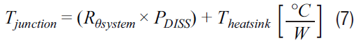
Be sure the calculated junction temperature does not exceed the max junction temperature of the component from the data sheet. The specified mean time to failure (MTTF) will be reduced significantly if the device is operated above the maximum junction temperature.
Conclusion
There have been many advances in semiconductor and electronic circuit technology. The demand for system designers to do more functions within the same or less space has brought forth some amazing integration and miniaturization techniques. Shoving more stuff into a smaller box has its consequences; the dissipated power in the form of heat has to be mitigated. This mitigation requirement has led to the development of very complex and very powerful thermal simulation software. These equations and findings are intended to help the system designer to get a quick, and fairly accurate sense of the thermal mitigation that would be required for the system. Hand calculation will never replace the thermal simulation tools—the intention of this discussion is to give the system designer a few simple tools to provide an early insight to the thermal mitigation requirement of their system design.
About the Authors
...
Related to this Article
Product Categories
{{modalTitle}}
{{modalDescription}}
{{dropdownTitle}}
- {{defaultSelectedText}} {{#each projectNames}}
- {{name}} {{/each}} {{#if newProjectText}}
-
 {{newProjectText}}
{{/if}}
{{newProjectText}}
{{/if}}
{{newProjectTitle}}
{{projectNameErrorText}}
Latest Media 21


