Alternate Circuits for Overvoltage Protection: Tips and Tricks
Abstract
Overvoltage protection (OVP) devices protect downstream circuits from overvoltage conditions that occur during load-dump events or transients. Sometimes the basic application circuit for an OVP device is not adequate for a particular application; here are two common variations. First, the circuit's maximum input voltage can be increased. Second, the circuit can be modified to use the output capacitor as a reservoir to hold energy during overvoltage or undervoltage conditions. This application note discusses how to make these two design modifications. The MAX6495–MAX6499/MAX6397/MAX6398 OVP devices serve as examples of the techniques.
Introduction
The MAX6495–MAX6499/MAX6397/MAX6398 overvoltage protection (OVP) devices protect downstream circuits from overvoltage conditions that occur during load-dump events or transients. The parts operate by controlling an n-channel MOSFET wired in series with the power rail. When the voltage surpasses a user-specified overvoltage threshold, the gate pulls low and the MOSFET shuts off, disconnecting the power rail.
The typical circuit presented in the data sheets for these OVP devices is suitable for most applications (see Figure 1). Occasionally, however, an application requires some modification of the basic circuit. Two such applications are discussed in this article: increasing the maximum input voltage, and using the output capacitor as a reservoir during an overvoltage event.
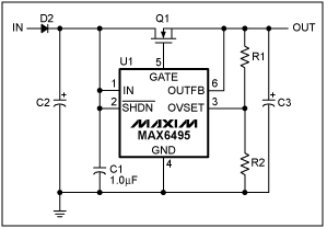
Figure 1. Basic overvoltage protector circuit.
Increasing the Maximum Input Voltage
Although the circuit in Figure 1 works for input-voltage transients up to 72V, some applications require more protection. It is thus advantageous to know how to increase the maximum input voltage in an OVP device. Figure 2 shows a circuit with an additional resistor and a zener diode which clamps the voltage on IN. While adding a transistor buffer (Figure 3) decreases the current requirement for the shunt regulator, it does increase design cost.
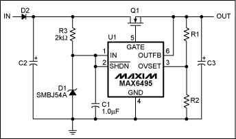
Figure 2. Overvoltage protector circuit that increases maximum input voltage.

Figure 3. This overvoltage protector circuit uses a transistor buffer to increase maximum input voltage.
To select the zener voltage and to avoid wasting power during normal operation, pick a voltage that is above the maximum normal input voltage. The zener voltage must, moreover, be below the maximum operating voltage of the OVP circuit (72V) during a transient condition where the current in the zener is highest.
The series resistor, R3, must be large enough to limit power dissipation in the zener diode during an overvoltage condition, but small enough to maintain power to the OVP IC with the minimum input voltage.
Calculating the R3 resistor value for Figure 2 begins with the following givens: the zener voltage of D1 is 54V; the overvoltage peak is 150V; and the power in the zener should be 3W or less. From this data, the maximum current flowing through the zener is:
3W/54V = 56mA
With this current, the lower limit of R3 should be:
(150V - 54V)/56mA = 1.7kΩ
Peak power dissipation in R3 is, therefore:
(56mA)² × 1.7kΩ = 5.3W
Resistor values smaller than this 5.3W will cause considerable power dissipation in the resistor and zener diode.
To calculate the resistor's upper limit, the minimum required power-supply voltage must be known. The MAX6495 requires an input voltage of at least 5.5V. In this example, the minimum power-supply voltage is 6V, therefore the acceptable voltage drop across resistor R3 during normal operation is 500mV. Since the supply current of the MAX6495 is 150µA(max), the corresponding maximum resistor value is:
500mV/150µA = 3.3kΩ
The resistor R3 for the circuit in Figure 2 was set at 2kΩ to ensure that the OVP device operates with input voltages slightly below 6V.
Note that significant power dissipates in R3 and D1 (Figure 2) during an overvoltage condition. If the overvoltage transient is sustained (i.e., longer than a few dozen milliseconds), the circuit in Figure 3 might be more appropriate for the application. This emitter-follower circuit far increases the allowable maximum value for R3 by reducing the current drawn from the node between R3 and D1. For a transistor β of 100, the 150µA supply current becomes 1.5µA. At this point, the diode's 5µA reverse leakage current cannot be neglected. R3 is set to 10kΩ, thus limiting the voltage drop on R3 caused by the leakage current to 50mV.
Use a 1µF (minimum) ceramic capacitor from IN to GND. Make sure that the voltage ratings of the components meet the input voltage requirements. Pay careful attention to the VDS_MAX rating of the series MOSFET.
Using the Output Capacitor as a Reservoir
During an overvoltage condition, the typical application circuit automatically discharges the output capacitor to protect downstream circuitry (Figure 4). Sometimes the application requires the output capacitor to store energy and maintain power to the downstream circuitry during a transient overvoltage condition. The circuit in Figure 5 implements this operation.
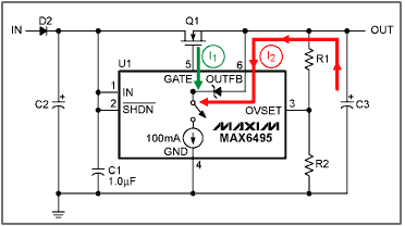
Figure 4. Typical overvoltage-limiter circuit showing the output capacitor's discharge path.
The MAX6495–MAX6499/MAX6397/MAX6398 use an internal 100mA current sink (see Figure 4) connected to the GATE output to discharge the gate capacitance and discharge the output capacitor. The current sink discharges the gate (see current I1, the green arrow), until the voltage on GATE equals the voltage on OUTFB. At this point the FET is turned off. The current sink continues to decrease the voltage on GATE, eventually forward biasing the internal clamp diode and discharging the output capacitance (current I2 in red).
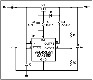
Figure 5. Overvoltage limiter with reservoir capacitor circuit.
If OUTFB is disconnected and thus removes the current path through the clamp diode, the output capacitor no longer discharges. However, the gate of the MOSFET no longer has the protective clamp diode and the VGS_MAX rating could be exceeded.
Adding an external clamp diode (D1 in Figure 5) from the source of the MOSFET to the gate of the MOSFET reintroduces the current path from the output to the 100mA current sink. By adding a resistor in series (R3 in Figure 5) between GATE and the gate pin, this current is limited and current drain on the output capacitor is reduced. Limiting the current can also increase the turn-off time and slow the circuit's response to sharp overvoltage transients. Adding a capacitor (C4 in Figure 5) across the series resistor helps decrease the response time. An optional resistor, R4, prevents OUTFB from floating.
If the MAX6495–MAX6499/MAX6397/MAX6398 operate in limiter mode by connecting the SET resistor-divider to the output connection instead of the input (see prior figures), the circuit can periodically add charge to the output capacitor. Then when the capacitor voltage drops below the hysteresis voltage of the overvoltage threshold, the series MOSFET turns on, charges the capacitor, and turns off when the voltage exceeds the overvoltage threshold.
Figure 6 shows the MAX6495–MAX6499/MAX6397/MAX6398 connected to operate in overvoltage monitoring mode. By connecting the SET resistor-divider to the input connection, the MOSFET will shut off during an input overvoltage and remain off until the overvoltage condition is removed.
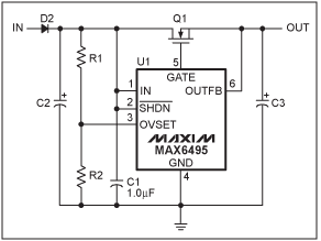
Figure 6. Overvoltage comparator configured in overvoltage monitoring mode.
Related to this Article
Products
PRODUCTION
72V, Overvoltage-Protection Switches/Limiter Controllers with an Exter...
72V, Overvoltage-Protection Switches/Limiter Controllers with an Exter...
PRODUCTION
Overvoltage Protection Switch/Limiter Controllers Operate Up to 72V
72V, Overvoltage-Protection Switches/Limiter Controllers with an Exter...
Overvoltage Protection Switch/Limiter Controllers Operate Up to 72V
72V, Overvoltage-Protection Switches/Limiter Controllers with an Exter...
72V, Overvoltage-Protection Switches/Limiter Controllers with an Exter...
Product Categories
{{modalTitle}}
{{modalDescription}}
{{dropdownTitle}}
- {{defaultSelectedText}} {{#each projectNames}}
- {{name}} {{/each}} {{#if newProjectText}}
-
 {{newProjectText}}
{{/if}}
{{newProjectText}}
{{/if}}
{{newProjectTitle}}
{{projectNameErrorText}}
Latest Media 21


