Abstract
This application note presents several benefits of using capacitors to AC-couple an LVDS data link. The article guides the reader through proper capacitor selection and termination topology. Common troubleshooting issues are discussed.
Introduction
Using capacitors to AC-couple an LVDS data link provides many benefits, such as level shifting, removing common-mode errors, and protecting against input-voltage fault conditions. This application note guides in the selection of both a proper capacitor and the termination topology for this design approach. Common troubleshooting issues are also discussed.
Level Shifting
LVDS (Low-Voltage Differential Signaling) logic inputs are one of many available logic standards. Using an AC-coupled link can offer the desired level translation, if the signal source provides sufficient amplitude for the LVDS inputs, which are typically 100mVP-P differential. Figure 1 depicts a negative ECL logic source that converts the signal levels to LVDS logic through such an AC-coupled link.

Figure 1. ECL-to-LVDS level-shifter configuration.
Optimal Common-Mode Voltage
AC-coupled LVDS also allows the receiving IC to set its optimal common-mode voltage. In Figure 2, a typical LVDS input is shown, in this case the MAX9248. An internal reference voltage, often 1.2V, biases two high-impedance termination resistors. If the inputs are AC-coupled, the receiving IC is allowed to set the common-mode voltage to its internal bias level.

Figure 2. LVDS input bias circuit.
Protecting from Overvoltage
LVDS signals are always AC-coupled in automotive serializer-deserializer (SerDes) links. Protecting the car's battery voltage from shorts is the primary motivation for this configuration. A universal requirement for any signal entering the wiring harness is that it must withstand a short-to-battery voltage without damage. With an AC-coupled LVDS link, there is only a brief pulse of high current as the coupling capacitors are charged to the battery voltage. The peak amplitude of the current is a function of the actual impedance of the short. The duration of the current spike is a function of the coupling capacitance and the protection structure of the LVDS input and output. Although the SerDes link is usually not functional during the short, operation can be restored once the short is removed.
Capacitor Selection
Several factors affect proper capacitor selection.
Value
The value of the AC-coupling capacitors used in the LVDS link depends on several parameters, including:
- Output Drive Level
- Input Threshold Level
- Load Impedance
- Cable Length
- Longest Pulse Duration
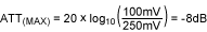
Consequently, the total attenuation from DC resistance, AC attenuation, and capacitive coupling droop must be less than -8dB. The load impedance is usually a 100Ω differential on both ends. Analyzing the cable length requires that both the cable's AC and DC attenuation plus losses from connector resistance all be considered.
Finally, the data itself must be considered. The longest pulse that the LVDS link must transmit is a function of the operating frequency and the maximum number of consecutive 1s (or 0s) that the data protocol will pass.
If all these calculations are too involved for an application, simply choose 0.1µF capacitors which will suffice for most applications. When the data rate drops below 10MHz or when longer cables lengths (i.e.,
Voltage and Dielectric
The operating voltage of the capacitors should be greater than the expected peak voltage during a fault condition. In automotive applications, the peak fault voltage is 18V. Double-fault conditions such as double battery voltage or load dump do not usually require consideration.
Use capacitors with X5R, X7R, or equivalent dielectric specifications. Avoid dielectrics with significant voltage and or temperature coefficients, such as Y5V or Z5U.
Termination Topology
The termination topology can be selected from three primary circuits: (1) pure differential; (2) center-tapped differential; and (3) Thevenin termination. Figure 3 shows these three circuits.

Figure 3. LVDS termination circuits.
Pure differential is the most common configuration, and works well for terminating signals in a well-shielded environment. The center-tapped differential termination splits the 100Ω termination into two 50Ω resistors, with a bypass capacitor at the center tap. This approach works well for noisy environments, as any common-mode energy induced on the LVDS pair sees a low impedance to ground. Both the pure differential and the center-tapped differential termination must be used with internally biased LVDS inputs.
If the LVDS receiver is not internally biased and if the input signal is AC-coupled, a Thevenin termination must be used. Select the resistors so that the Thevenin impedance on each line is 50Ω and that the Thevenin voltage on each line is 1.2V. The values in Figure 3 work for a 3.3V supply.
Troubleshooting AC-Coupled Links
The data transmitted over an AC-coupled LVDS link must be DC-balanced, which means that the number of 0s transmitted must be as close as possible to the number of 1s transmitted. Clock signals of nominally 50% duty cycle are intrinsically DC-balanced. Many data encoding algorithms, such as Manchester encoding, also provide DC-balanced data streams. Figure 4 depicts the plot of a link without DC-balance.

Figure 4. AC-coupled LVDS link without DC-balance.
The top traces in Figure 4 (red and blue) reflect the single-ended measurement of a 20% duty-cycle pulse stream. The bottom trace (green) is a differential measurement across both complementary and true signals. The differential measurement is not centered on 0V and is skewed. A careful analysis shows that the area under each half of the waveform is equal. The AC-coupled link is unable to transmit any DC current. For this case, the negative excursion is just below 100mV, violating the LVDS minimum input levels.
Fail-Safe Inputs
Some LVDS devices have a fail-safe circuit on their inputs. A fail-safe circuit identifies input faults; it disables the output driver if a fault is detected. The MAX9180 low-noise LVDS repeater is an example of this design, and shown in Figure 5. If an AC-coupled LVDS link is attempted with a fail-safe circuit, a Thevenin termination of the inputs is required. If this configuration is not used, the DC voltage at the inputs is almost VCC, which is outside the common-mode voltage range for the LVDS device.

Figure 5. LVDS fail-safe input circuit.
A similar article was published on the Planet Analog website by CMP Media LLC, October 2, 2007.
Related to this Article
Product Categories
{{modalTitle}}
{{modalDescription}}
{{dropdownTitle}}
- {{defaultSelectedText}} {{#each projectNames}}
- {{name}} {{/each}} {{#if newProjectText}}
-
 {{newProjectText}}
{{/if}}
{{newProjectText}}
{{/if}}
{{newProjectTitle}}
{{projectNameErrorText}}
Latest Media 21


