24-Bit ADC Challenges ΔΣ Conventions
Introduction
Using a delta sigma ADC for precision instrumentation can be a simple proposition, despite conventional wisdom to the contrary. Conventional wisdom suggests that measuring low level signals, such as strain gauge bridges or thermocouples, requires amplification to match the ADC input range. Conventional wisdom also suggests that achieving a high level of accuracy and rejection requires a fast output rate and accompanying post-processing, and that a low impedance source cannot be measured directly, but requires buffering. The natural conclusion of conventional wisdom is that high resolution, delta sigma ADCs make for complex designs. Conventional wisdom may be conventional, but in this case it is not necessarily wise.
Analog Devices has produced an extensive family of ultrahigh precision delta sigma analog-to-digital converters. This family differentiates itself from other high resolution converters by offering extreme accuracy without the added complexities usually associated with delta sigma converters. Calibration sequences, configuration registers, filter settling time, and external oscillators are eliminated. Transparent offset and full-scale auto calibration are performed every conversion cycle to ensure absolute accuracy independent of time, temperature, and supply voltage. The No Latency Delta-Sigma™ architecture simplifies multiplexing applications. An internal oscillator enables accurate line frequency rejection while eliminating the need for high frequency external oscillators and the coupling problems that can result.
Figure 2 shows a block diagram of the new LTC2440, which uses a new delta sigma converter architecture but remains pin and timing compatible with the existing delta sigma converter product line. A programmable over sample ratio (OSR) allows users to tune the speed and resolution for a variety of applications (see Figure 1). Figure 3 shows the ten speed/resolution combinations from 6.9Hz/24.6 bits to 3.5kHz/17 bits which are selectable through a simple serial interface, where resolution = log(RMS noise/5)/log 2. The digital filter has no latency, allowing the converter to respond to speed selections or external input channel changes between conversions without settling errors.

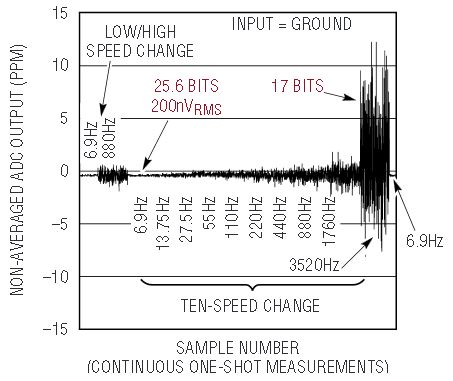
Figure 1. Shifting gears on the LTC2440 has little to no affect on accuracy. This graph shows continuous single-shot measurements of a grounded input as the speed is changed on the fly. The speed change from 6.9Hz to 880Hz is implemented by simply driving the SDI pin from low to high. Alternatively, the speed can be increased in nine steps (5-bit input to SDI) from 6.9Hz to 3.5kHz.


Figure 2. High performance variable speed/resolution ΔΣ architecture.

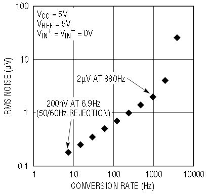
Figure 3. The variety of easy-to-select speed/resolution combinations allows the LTC2440 to be tailored to many applications.
The ultra low noise of the ADC eliminates the system-level complexities related to using PGAs by offering 25 million counts over a ±2.5V input range (200nVRMSNOISE) or 500,000 counts over a ±50mV input range independent of sensor offset/tare voltages. The absolute accuracy (5ppm INL, 1ppm offset, 10ppm full-scale, all independent of output rate), and flexible input range (common mode input from GND to VCC independent of VREF) greatly simplify analog front end circuitry.
Measuring Low Level Signals without a PGA
Programmable gain amplifiers (PGAs) are commonly used in systems where a small input signal (RTD, thermocouple, strain gauge) needs to be applied to a wide input range analog-to-digital converter. The convention is to amplify the sensor output voltage range so that it matches the ADC input range. The input referred noise due to the ADC is reduced by the PGA gain. However, the system performance is dominated by the noise performance of the PGA as well as its offset, full-scale, and linearity performance. PGAs degrade the system performance by introducing added error sources, drift, cost and complexity. In addition, sensor offset/tare voltages need to be adjusted out to prevent saturating the amplifier output or over-ranging the ADC input. Because PGAs are used to reduce the noise contributed by the analog-to-digital converter, if the ADC noise is low enough, these PGA tradeoffs can be eliminated.
Eliminating the PGA (and tare adjust) requires a converter with exceptional offset, linearity, full-scale accuracy, drift, and noise performance. The converter requires enough resolution over its full input range to maintain high resolution within a significantly reduced portion of its input span. This allows system designers to directly interface sensors to the ADC while using a small portion of the overall converter input range; thus, significantly simplifying the analog front end. The number of counts produced over the full output range typically determines performance. The resolution is determined by dividing the sensor’s full-scale output voltage by the RMS noise of the analog front end.
The LTC2440 running at 6.9Hz has an RMS noise level of 200nV over a ±2.5V input range equivalent to 25,000,000 counts. The exceptional noise performance of this device allows the user to make one conversion (no averaging) with 500,000 counts and no DC errors for any ±50mV range (Figure 4). Because it doesn’t need a PGA, the LTC2440 maintains a wide input range and easily handles sensor offset and tare voltages. The offset error is less than 5μV independent of temperature and the full-scale is within 0.003% with less than 0.2ppm/C drift.


Figure 4. High resolution mode directly digitizes low level signals even while monitoring a wide input range.
The exceptional DC performance of the LTC2440 does not require extra system calibration. The programmable OSR enables the system to seamlessly change the conversion rate without degrading this exceptional DC performance. While running at 880Hz, the LTC2440 maintains approximately 50,000 counts over the same ±50mV range. Then the OSR can be changed to 6.9Hz on the next conversion with full accuracy, as shown in Figure 1. The OSR is programmed either by tying a single pin LOW or HIGH (880Hz or 6.9Hz) or with a 5-bit serial word applied to that same pin (10 speed selections).
The offset, full-scale, integral linearity and power dissipation are all independent of the speed selected. Speed independent accuracy coupled with no latency enables users to gear shift between conversions. For example, the LTC2440 may monitor a fast moving signal at 3.5kHz output rate, and then switch to a slower output rate in order to obtain a lower noise reading. This is useful in systems monitoring input perturbations as they settle, auto-ranging circuits, or general data acquisition.
Achieving High Input Rejection without High Output Rates
One property common to all high resolution delta sigma ADCs is an on chip digital lowpass filter. These filters offer excellent rejection up to the internal modulator sampling rate. At multiples of the internal modulator sample rate, unwanted input perturbations are folded back to DC with little attenuation (aliasing). Delta sigma converters sample the input at a multiple, commonly referred to as the over sample ratio (OSR), of the output rate. Since the OSR is typically large (≥64), the digital filter offers excellent rejection of input noise sources and simple antialiasing requirements.
Conventional high resolution delta sigma ADCs operate at a fixed OSR typically between 64 and 256. In order for these devices to reject 50Hz and 60Hz line frequencies the modulator sample rate, fSAMPLE, is only 64 to 256 times the line frequency (3.8kHz to 15.3kHz). Noise applied to the input with frequency content at fSAMPLE is aliased back to DC resulting in unwanted errors. As the OSR is increased for a given rejection frequency, fSAMPLE is increased and the antialiasing requirements are reduced.
The LTC2440 internal sampling clock (fSAMPLE) is fixed at 1.8MHz independent of the output rate. In order to change the output rate, the internal OSR is changed. While the LTC2440 is operating at 6.9Hz, the digital filter simultaneously rejects 50Hz and 60Hz and the OSR is very high (32,768). With its sample rate of 1.8MHz, the LTC2440 offers much more rejection and simple antialiasing compared to conventional converters running at lower OSRs, as shown in Figure 5.

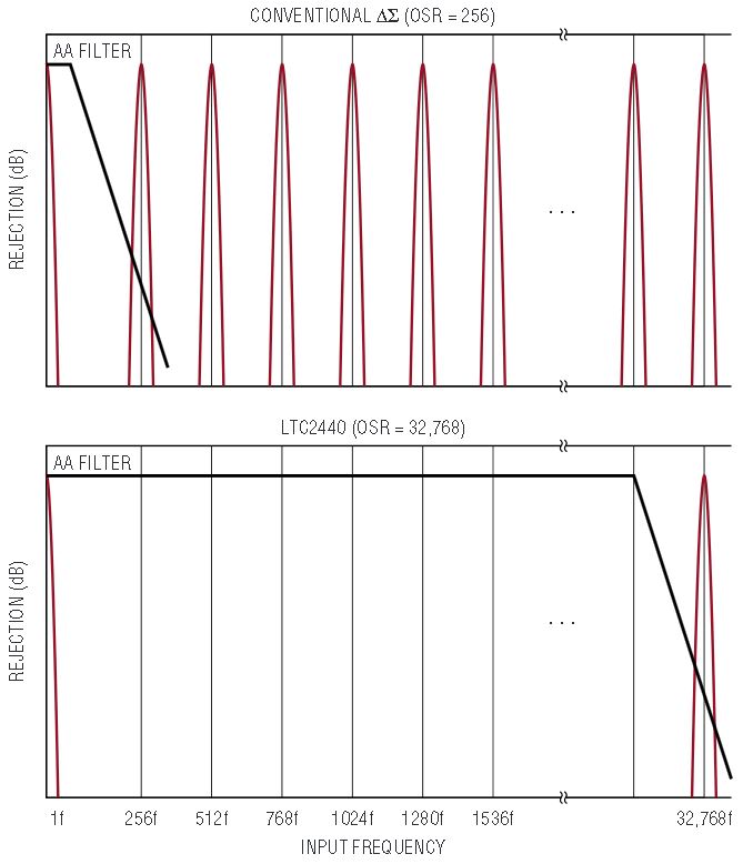
Figure 5. Large OSR eases front end filtering requirements.
Direct Digitization of Low Level Signals without Buffers
A commonly overlooked and/or misunderstood issue related to analog-to-digital converters is the effect of the switched-capacitor sampling network on performance. Looking into the input terminal of a delta-sigma converter is a high frequency switched capacitor array switching at a frequency, fSAMPLE. If the external network tied to the converter input settles within the sampling period (1/fSAMPLE), no error results. The source impedance of the sensor, external capacitance at the input terminal, the ADC sample rate, and the size of the internal sampling capacitor determine the settling time.
Some manufacturers of high resolution delta-sigma converters have invented various clever ways to improve the apparent input settling, but the tradeoffs in system performance render these methods impractical for many applications. Some include on-chip buffers in the signal path to isolate the switched capacitor array from the external circuit. The problem with this approach is the input signal range is limited to several hundred millivolts above ground and 1.5V below VDD. Since many sensors’ output ranges are outside of this range, these buffers cannot be used. Other manufacturers attempt to solve this problem by partially sampling the output of the buffer through a coarse cycle, then sampling the residual through a fine sample. While this allows input signals near ground, it introduces settling errors as a function of the amplifier’s offset and common mode rejection. This results in signal dependent errors that vary over time and temperature.
For these reasons, most system designers choose to disable the input buffer circuitry and handle the input settling externally. Some designers have discovered when they remove the bypassing capacitor at the input to the ADC and apply the sensor directly to the converter the input settling errors are gone. In this case, the input settling errors are no longer a function of the large external capacitor, but become a function of the external source resistance and the internal sampling capacitor (typically on the order of a few pF).
The LTC2440 can directly digitize sensors with output impedances up to 500Ω with no errors due to the input settling current. This allows direct digitization of thermocouples, RTDs, and 350Ω bridges. In the case of remote sensing, the LTC2440 can be directly connected to the sensor. The excellent common mode and normal mode input rejection enables direct connection without the need for external amplifiers, level shifters, and capacitors. Since the programmable OSR technology adjusts the output rate without changing the internal sampling rate, the input settling characteristics are independent of conversion rate. Thus, a 500Ω source impedance signal can be measured at any output rate from 6.9Hz to 3.5kHz while the output level and input settling characteristics do not change.
Running with a Slow External Oscillator
fSAMPLE is set to 1.8MHz by a factory-tuned on-chip oscillator running at 9MHz. This oscillator may be overridden by attaching an external oscillator to the device. If the external oscillator is set to 100kHz, for example, the internal sample rate is reduced to 20kHz. While this internal sample rate is on the order of conventional delta sigma converters offering great input rejection at 60Hz, the LTC2440 rejects frequencies above 0.6Hz (see Figure 6). This is equivalent to an impractical lowpass filter with external resistances on the order of MΩ or capacitances on the order of Farads. In addition to rejection above 0.6Hz, the LTC2440 front end analog circuitry incorporates a chopper which removes the very low frequency 1/f noise and offset drift. Under these conditions, the LTC2440 can be used to precisely measure DC voltages in excessively noisy environments.

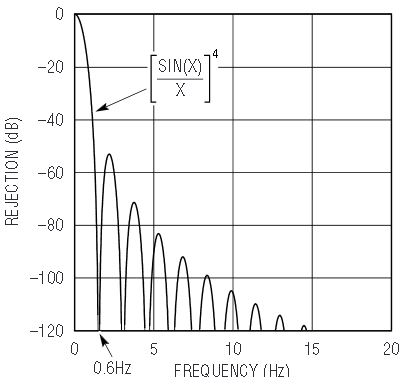
Figure 6. Input rejection with an external 100kHz oscillator reduces noise down to 0.6Hz.
One such application is measuring the DC current through a shunt resistor (see Figure 7). Any noise above 0.6Hz is rejected by more than 120dB up to the sample rate. Since the OSR is large (32,768), the antialiasing requirements are simple. Other delta-sigma converters using low OSRs for their digital filter sample the input at rates below 150Hz making antialiasing extremely difficult.

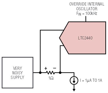
Figure 7. Very low frequency rejection and wide common mode input range enable precise current sensing over a wide current range.
Running with an external oscillator of 100kHz and the highest resolution (OSR = 32,768), the RMS noise of the LTC2440 is 200nV over a full ±2.5V input range. Six decades of current, in either direction, can be measured accurately through a 1Ω resistor independent of low frequency system noise. The flexible common mode input range enables the LTC2440 to digitize these signals near VDD.
Reduced Power Operation
In addition to adjusting the speed/resolution of the LTC2440, the average power dissipation may also be adjusted using the automatic sleep mode. During the conversion cycle, the LTC2440 draws 8mA independent of the conversion output rate. Once the conversion is completed, the device automatically enters a low power sleep state drawing 8μA. The device remains in this state until the conversion result is read. The user may reduce the DC power dissipation by extending the duration of the low power sleep state.
For example, if the OSR (OSR = 64) is programmed for minimum conversion rate (TCONV = 0.285ms) and the sleep state is extended to 10ms, the effective output rate is 100Hz while the power dissipation is below 1.3mW. By further extending the duration of the sleep state to 100ms, the effective output rate is 10Hz and the power dissipation is 150μW. Noise, power, and speed can be adjusted by setting the OSR and sleep mode duration.
Summary
The LTC2440 offers accuracy, stability, and ease of use that are common to the LTC2400 product family. It combines a programmable OSR digital filter with a high speed analog modulator in order to achieve high speed and accuracy independent of output rate. The LTC2440’s wide range of user programmable speed and resolution combinations makes it flexible enough to fit in a wide variety of applications.
About the Authors
Related to this Article
{{modalTitle}}
{{modalDescription}}
{{dropdownTitle}}
- {{defaultSelectedText}} {{#each projectNames}}
- {{name}} {{/each}} {{#if newProjectText}}
-
 {{newProjectText}}
{{/if}}
{{newProjectText}}
{{/if}}
{{newProjectTitle}}
{{projectNameErrorText}}
Latest Media 21


