MAXREFDES48


Overview
Design Resources
Design & Integration File
- Schematic
- PCB Layout
- BOM
- PCB Gerber
- PCB CAD (PADS 9.0)
Evaluation Hardware
Part Numbers with "Z" indicate RoHS Compliance. Boards checked are needed to evaluate this circuit.
- MAXREFDES48# ($51.09) EV Kit
Description
Introduction
Note: This reference design uses an EFD20 core transformer. For the similar reference design using a planar transformer, refer to the MAXREFEDES41.
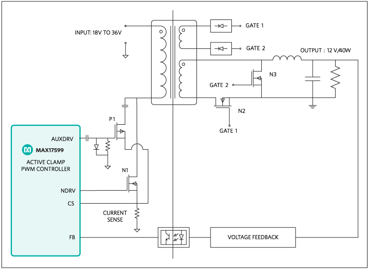
The MAXREFDES48 reference design (Figure 1) demonstrates the application of the MAX17599 low IQ, wide-input range, active clamp current-mode PWM controller. The MAX17599 contains all the control circuitry required for the design of wide-input isolated forward-converter industrial power supplies. The reference design operates over an 18V to 36V input voltage range, and provides up to 3.5A at 12V output. The reference design features the active-clamp transformer reset topology for forward converters. This reset topology has several advantages including reduced voltage stress on the switches, transformer size reduction due to larger allowable flux swing, and improved efficiency due to elimination of dissipative snubber circuitry. These features result in a compact and cost-effective isolated power supply. The design is set to switch at 250kHz. For EMI-sensitive applications, the user can program the frequency-dithering scheme, enabling low-EMI spread-spectrum operation.
The input undervoltage lockout (EN/UVLO) is provided for programming the input-supply start voltage (set to 16.5V in the design) and to ensure proper operation during brownout conditions. The EN/UVLO input is also used to turn on/off the IC. The overvoltage input (OVI) protection scheme is provided to make sure that the controller shuts down when the input supply exceeds its maximum allowed value (set to 37.0V in the design).
To control inrush current, the device incorporates a soft-start (SS) pin to set the soft-start time for the regulator. Power dissipation under fault conditions is minimized by hiccup overcurrent protection (hiccup mode). The soft-stop feature provides safe discharging of the clamp capacitor when the device is turned off, and allows the controller to restart in a well-controlled manner.
Additionally, the negative current limit is provided in the current-sense circuitry, helping limit clamp switch current under dynamic operating conditions. An overtemperature fault triggers thermal shutdown for reliable protection of the device.
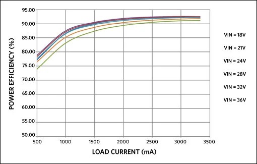
The reference design delivers a peak efficiency of 92.5% with the supplied components when the input is 24V. This general-purpose power solution can be used in many different types of power applications, such as programmable logic controllers (PLC), industrial process control, industrial sensors, telecom/datacom power supplies, isolated battery chargers, servers, and embedded computing.
Parts Used
Details Section


Documentation & Resources
-
MAXREFDES48 Design Files2/17/2021ZIP1 M
Support & Training
Search our knowledge base for answers to your technical questions. Our dedicated team of Applications Engineers are also available to answer your technical questions.