Designed, Built, Tested
Board pictured here has been fully assembled and tested.

Overview

Design Resources

Design & Integration File

  • Schematic
  • Bill of Material
  • PCB Layout
Download Design Files 1.13 M

Evaluation Hardware

Part Numbers with "Z" indicate RoHS Compliance. Boards checked are needed to evaluate this circuit.

  • MAXREFDES281# IO-Link Data Link Controller Reference Design with PMOD Connector
Check Inventory & Purchase

Device Drivers

Software such as C code and/or FPGA code, used to communicate with component's digital interface.

MAX22516 GitHub No-OS Driver Source Code

Description

Advanced factory automation solutions (i.e., Industry 4.0) require an increasing number of smart sensors and smart actuators, which are typically controlled using IO-Link® point-to-point serial communication between the sensor/actuator and IO-Link master. As a leading provider of IO-Link device transceiver and master transceiver ICs, Analog Devices, Inc., also provides complete reference design solutions to help our customers improve their time to market. These proven designs cover all the hardware and software requirements needed for compliance with the IO-Link standard.

IO-Link is the first open, field bus agnostic, low-cost, point-to-point serial communication protocol used for communicating with sensors and actuators that has been adopted as an international standard (IEC 61131-9). IO-Link standardizes interoperability of industrial equipment from all over the world. IO-Link can function directly from a PLC or be integrated into standard field buses, quickly making it the de-facto standard for universally communicating with smart devices like the MAXREFDES281#.

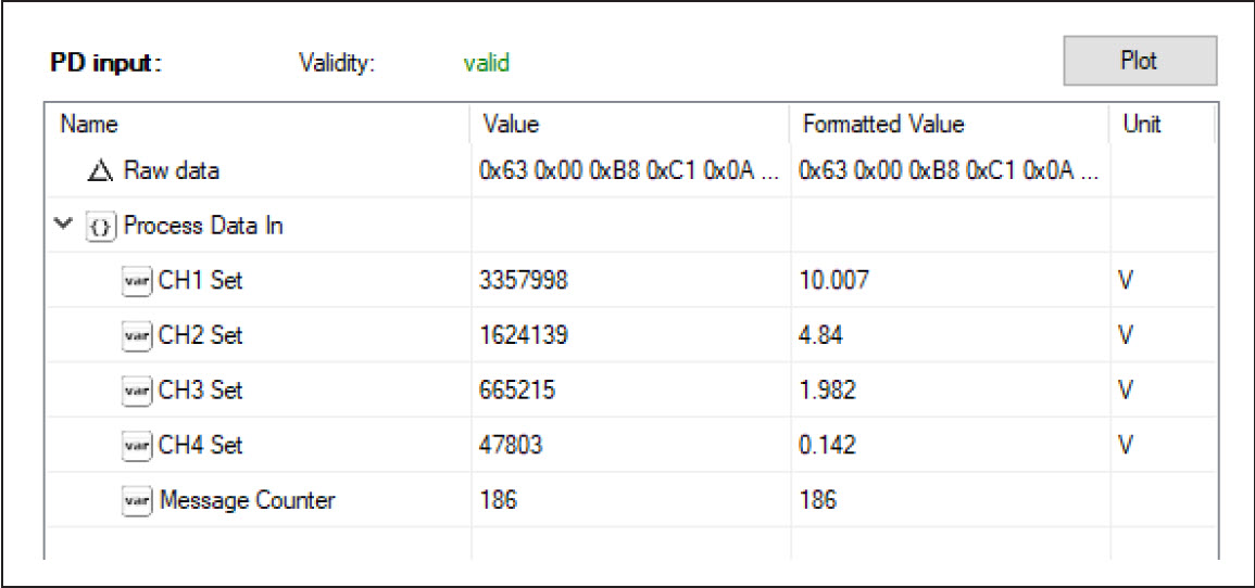
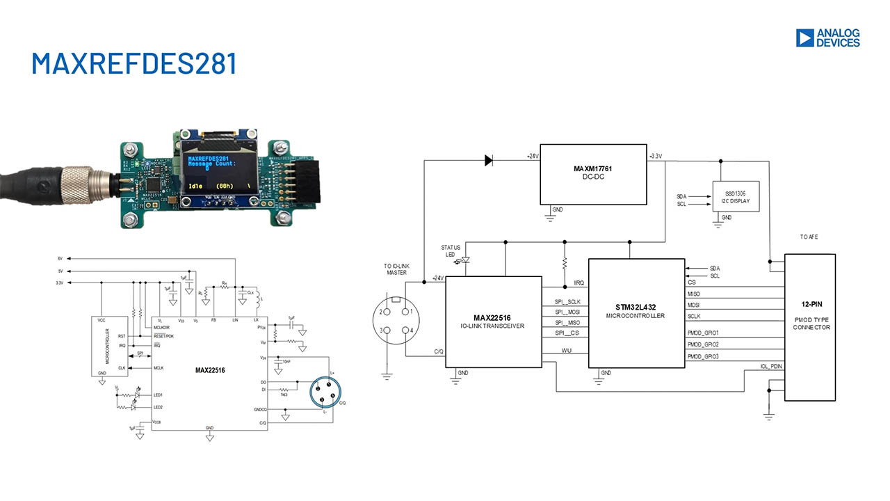
The MAXREFDES281# is a complete, IO-Link reference design that allows an engineer to connect device or actuator development boards with a Pmod-compatible peripheral module connector, and interface to an IO-Link Master. The MAXREFDES281# consists of a MAX22516 IO-Link transceiver with integrated data link controller and protection, a microcontroller to run application code, and has a peripheral module connector to connect device or actuator functions, supporting SPI, I2C, or UART interfaces.

The complete reference design fits on a 75mm x 33mm printed circuit board (PCB). Design files and software are available on the Design Files folder. The board is also available for purchase.

Features & Benefits

  • IEC 61131-9-Compliant
  • IO-Link Version 1.1-Compliant

Parts Used

Details Section

With this reference design and firmware, IO-Link allows the user to program and diagnose a four-channel industrial analog input peripheral module (MAX22005PMB#), or a four-channel industrial analog output peripheral module (MAX22007PMB#). This enables industrial actuator or sensor equipment OEMs to provide end-users with total flexibility at the factory floor level to simplify equipment installation and commissioning, while reducing their own number of stock keeping units, reducing their BOMs, simplifying and streamlining their own purchasing and manufacturing.

The demonstration firmware provides following three example options to use the MAXREFDES281#:

  1. A Display Demo supporting 2-byte PDIn and 1-byte PDOut, where this demo shows a 32-bit message counter on the display and provides the same data through PDIn process data. The minimum cycle-time is defined by the process-data length and the COM rate, with this mode 500μs cycle-time can be reached. The PDOut byte allows to switch the display through different modes, i.e., timing analysis and application vs. cycle-time measurements.
  2. A MAX22007PMB# Demo supporting 1-byte PDIn and 7-byte PDOut, where the PDIn data is used as an 8-bit message counter, the 7-byte PDOut is split into 4x 12-bit DAC values, one for each analog output, and 1 byte to switch the display through different modes, i.e., application data display, timing analysis vs. cycle-time measurements. The minimum cycle-time is defined by the process-data length and the COM rate, with this mode 900μs cycle-time can be reached. The MAX22007PMB# demonstrates four industrial analog outputs that can be individually configured between voltage mode (0–12.5V) or current mode (0–25mA).
  3. A MAX22005PMB# Demo supporting 13-byte PDIn and 1-byte PDOut, where the PDIn data consists of 4x 24-bit values raw data from the ADC plus 1-byte message counter, and the 1-byte PDOut allows to switch the display through different modes, i.e., application data display, timing analysis vs. cycle-time measurements. The minimum cycle-time is defined by the process-data length and the COM rate, with this mode 1300μs cycle-time can be reached. The MAX22005PMB# demonstrates four industrial analog inputs that can be individually configured between voltage mode (0–12.5V) or current mode (0–25mA).

Built in an industrial form factor, and measuring just 75mm x 33mm, the MAXREFDES281# uses an industry-standard M12 connector, allowing a 4-wire IO-Link cable to be used. On the other side, a 12-pin peripheral module can be connected. A 2-pin terminal block provides external access to the 24V that is delivered from the IO-Link master, providing up to 24W.

The three demo applications come with matching Input/Output Device Descriptor (IODD) files, supporting multiple parameters to allow to configure different modes.

In this reference design, an STM32 low-power microcontroller interfaces between the MAX22516 and the peripheral module connector. The MAX22516 features an integrated data link controller which allows the device to autonomously respond to process-data requests from the IO-Link Master as well as manage indexed service data unit (ISDU) transfers, offloading all time-critical tasks from the microcontroller.

The microcontroller can update and read the PDIn and PDOut data at any time. The ISDU requests are stored in a separate FIFO and, consequently, are handled without interrupting application tasks. The MAX22516 also integrates surge protection for robust communication without requiring external protection components such as TVS diodes. The MAX22516 is available in a form factor friendly 3.53mm x 3.16mm, 42-bump Wafer Level Packaging (WLP) as well as a 40-pin TQFN package, allowing the MAXREFDES281# to have a small footprint. The reference design is reverse-polarity protected using the integrated active reverse-polarity protection of the MAX22516. The MAX22516 has an integrated DC-DC converter as well as two integrated linear regulators (3.3V and 5.0V). The DC-DC converter is used to generate the 3.3V supply for the microcontroller, reducing power dissipation as well as the number of external components required further saving additional space on the board. The MAX22516 also features a low on-resistance C/Q driver to reduce power dissipation, allowing this reference design to consume minimal power with very low thermal dissipation.

This IO-Link device was tested to IO-Link Standard 1.1.3 using the TEConcept Device Tester. Connecting the MAXREFDES281# to a USB IO-Link master, such as the MAXREFDES165# or MAXREFDES145#, with the associated software allows for easy evaluation.

Figure 2. MAXREFDES281# system block diagram
Figure 2. MAXREFDES281# system block diagram.

Detailed Description of Hardware

The MAXREFDES281# IO-Link to peripheral module device uses minimal power, space, and minimizes cost, making it a complete solution for many sensors and actuators found in various industrial control and automation applications.

The MAX22516 IO-Link device transceiver is compliant with the IO-Link version 1.1/1.0 physical layer specification. It integrates the high-voltage functions commonly found in industrial sensors and actuators, including drivers, DC-DC converter, and two linear regulators. The MAX22516 features extensive integrated protection to ensure robust communication in harsh industrial environments. All three I/O pins (V24, C/Q, and GND) on the MAX22516 are reverse-voltage and short-circuit protected and feature integrated ±1kV/500Ω surge protection. This enables a very small PCB area with no external protection components required. The low on-resistance driver (C/Q) further reduces power dissipation so this reference design consumes minimal power with very low thermal dissipation. Operation is specified for normal 24V supply voltages up to 36V. External transient protection is simplified due to the high voltage tolerance (i.e., 65V absolute maximum rating) for the I/O pins in addition to the integrated surge protection.

The integrated DC-DC regulator in the MAX22516 generates the 3.3V supply for the microcontroller, reducing the number of additional external components and the required space.

An additional MAXM17761 DC-DC converter module on the PCB provides 3.3V to the PMOD style connector, allowing currents of up to 1A for the connected peripheral module.

The MAX22516 features an integrated data link controller that significantly simplifies the IO-Link communication timing requirements with independent buffers for PDIn, PDOut, and ISDU transfers. The microcontroller can read or write to/from the buffers as the application allows, independent from the IO-Link Master timing.

Description of Firmware

The MAXREFDES281# ships preprogrammed as a working IO-Link device ready to connect to an IO-Link master. The firmware configures and controls a peripheral module. After plug-in, the MAXREFDES281# waits for a wake-up signal from the IO-Link master. Once the wake-up signal is received, the MAXREFDES281# synchronizes with the IO-Link master using the 230.4kbps (COM3) baud rate, and communication parameters are exchanged. The IO-Link master then starts a cyclic data exchange by transferring the process data. If the MAXREFDES281# is removed, the IO-Link master detects a missing device.

Figure 3. MAXREFDES145# + MAXREFDES281# + MAX22007PMB#.

The MAXREFDES145# is an eight-port IO-Link Master utilizing the TEConcept IO-Link Master Stack. The TEConcept IO-Link Control Tool software is Windows®-compatible and features IODD file import capability, automatic download from IODD Finder, connects to a PC through USB, and is available to download from the Analog Devices website.

The TEConcept IO-Link Control Tool software is shown in Figure 4.

Figure 3. MAXREFDES145# + MAXREFDES281# + MAX22007PMB#.

Detailed Description of Software

The MAXREFDES281# was verified using the MAXREFDES145# IO-Link Master, featuring the MAX14819 IO-Link master transceiver and the IO-Link Control Tool from TEConcept.

Download the IODD file (*.xml) located in the Design Files folder and follow the step-by-step instructions in the Quick Start Guide section on how to use the software. Figure 4 shows a screenshot of the TEConcept IO-Link Control Tool communicating with the master and device.

Restrictions and Warnings for ADI Reference Design Use

The MAXREFDES281# is designed and tested to meet IO-Link operation and harsh industrial environments covered by IEC 61000-4-x standards for transient immunity. This board and associated software are designed to be used to evaluate the performance of the MAX22516 but are not intended to be deployed as-is into an end product in a factory automation system.

The MAXREFDES281# is not for use in functional safety or safety-critical systems.

Figure 4. The TEconcept IO-Link control tool.

To test the MAXREFDES281#, connect it to a port of an IO-Link master. In the following example, a MAXREFDES145# IO-Link master and TEConcept IO-Link Control Tool are used, but any IO-Link-compliant master and associated IO-Link device GUI should work.

Required Equipment

Supplied by ADI
  • MAXREFDES281#
Note: Download IODD files from the Design Files folder.
User Supplied
  • IO-Link master (i.e., MAXREFDES145#) with a 24V AC-to-DC power adapter
  • TEConcept IO-Link Control Tool software
  • One IO-Link cable
  • Windows PC with one USB 2.0 Type B cable
Master Setup Procedure
  1. Connect the MAXREFDES281# to the IO-Link master with an IO-Link M12 cable.
  2. Connect the IO-Link master to the PC with a USB cable.
  3. Download and install the latest IO-Link Control Tool software from the Analog Devices website.
  4. Download the IODD file for the MAXREFDES281# either from the Design Files folder or from the IODD Finder website.
  5. The MAXREFDES281# comes preprogrammed with firmware that supports:
    1. MAX22007PMB# Mode
    2. MAX22005PMB# Mode
    3. Display Demo Mode
MAXREFDES281# Testing Procedure

The MAXREFDES281# supports the following three options:

  • Four-channel analog output using the MAX22007PMB#. To use this option, connect the MAX22007PMB# to MAXREFDES281# prior to providing 24V from the IO-Link master.
  • Four-Channel Analog Input using the MAX22005PMB#. To use this option, connect the MAX22005PMB# to MAXREFDES281# prior to providing 24V from the IO-Link master.
  • IO-Link Master cycle-time display. To use this option, make sure nothing is connected to the Pmod connector when 24V is applied from the IO-Link master.

Testing Procedure - Four-Channel Analog Output Using MAX22007PMB#

  1. Connect the female end of the IO-Link cable to the MAXREFDES281# (see Figure 3).
  2. Connect the male end of the IO-Link cable to one of the ports on the IO-Link master. For this procedure, we will use the MAXREFDES145# as the IO-Link master.
  3. Make sure that the MAXREFDES145# is powered with 24V supply and connected to the PC through a USB cable.
  4. Open the IO-Link Control Tool software and press the Refresh button under FTDI USB-SPI Interfaces. The GUI automatically finds the IO-Link master. Then, click the green Connect button.

  5. Import the IODD file (MAXIM-RD281_MAX22007PMB_COM3, MAXIM-RD281_MAX22005PMB_COM3 and MAXIM-RD281_DisplayDemoCOM3) for the MAXREFDES281#. The TEConcept GUI also allows to automatically download the IODD file from the IODD Finder by clicking the button IODD Finder in the Select Device menu.

  6. In the Device Tree on the left side, select the Port where the MAXREFDES281# is connected to.
  7. Click the Power ON button and this enables the L+ supply for the selected Port. The power-led on MAXREFDES281# as well as the red L+ LED on the selected MAXREFDES145# Port should now be on.

  8. Then, click the IO-Link button.
  9. If communication is established correctly, the IO-Link Control Tool software shows the Vendor ID, Device ID, Cycle time, as well as the Process Data input (PD input).
    Next to PD input, it should show “Validity: valid” in green. This means the Master is successfully communicating with the IO-Link device.

  10. If the MAX22007PMB# is connected at power-up:
    1. The MAXREFDES145# automatically detects this and opens the appropriate IODD:

    2. The PDIn shows an 8-bit message counter:

    3. The PDOut allows to set the output level on the four individual channels as well as an application mode:

    4. In PDOut, there is also a Mode selection that allows to change the display mode on the fly to show either Application Specific input (i.e., Voltage and Current settings) or some IO-Link statistics or Timing Analysis.

    5. The individual channel mode (Voltage/Current) can be set up in the Parameter Menu under “Channel Output Modes.”

    6. Channels can be switched on (Active) or off (High-Z) under “Channels On/Off.”

  11. If the MAX22005PMB# is connected at power-up:
    1. The MAXREFDES145# automatically detects this and opens the appropriate IODD:

    2. The PDIn shows a 24-bit analog value for each of the four channels. It can be either voltage or current as selected in the Parameter menu. Also, an 8-bit message counter is displayed there.

    3. The PDOut allows to select a mode for the display that allows to change the display mode on the fly to show either Application Specific input (i.e., Voltage and Current settings) or some IO-Link statistics or Timing Analysis.

    4. The individual channel mode (Voltage/Current) can be set up in the Parameter Menu under “Channel Input Modes.”

    5. Channels can be switched on (Active) or Off under “Channels On/Off” menu. Channels that are “Off” are not sampled by the ADC, so there is less switching of the integrated MUX and the resulting sample rate for the active channels is higher.

  12. If no peripheral module is connected at power-up:
    1. The MAXREFDES145# automatically detects this and opens the appropriate IODD for the display demo mode.

    2. This is a demo for short cycle time (as low as 500μs with PDIn and PDOut).
      There is 2-byte PDIn, this is a 16-bit Message counter as well as 1-byte PDOut.
      The message counter runs internally with 32 bits so the display shows the entire message count, while the PDIn provides only the 2 least significant bytes of the counter to allow for shorter cycle time.
    3. The PDOut byte contains a mode selection, which allows to select the mode on the fly to show either Application Specific input (i.e., the 32-bit Message counter) or some IO-Link statistics or Timing Analysis.

Support & Training

Search our knowledge base for answers to your technical questions. Our dedicated team of Applications Engineers are also available to answer your technical questions.