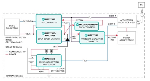
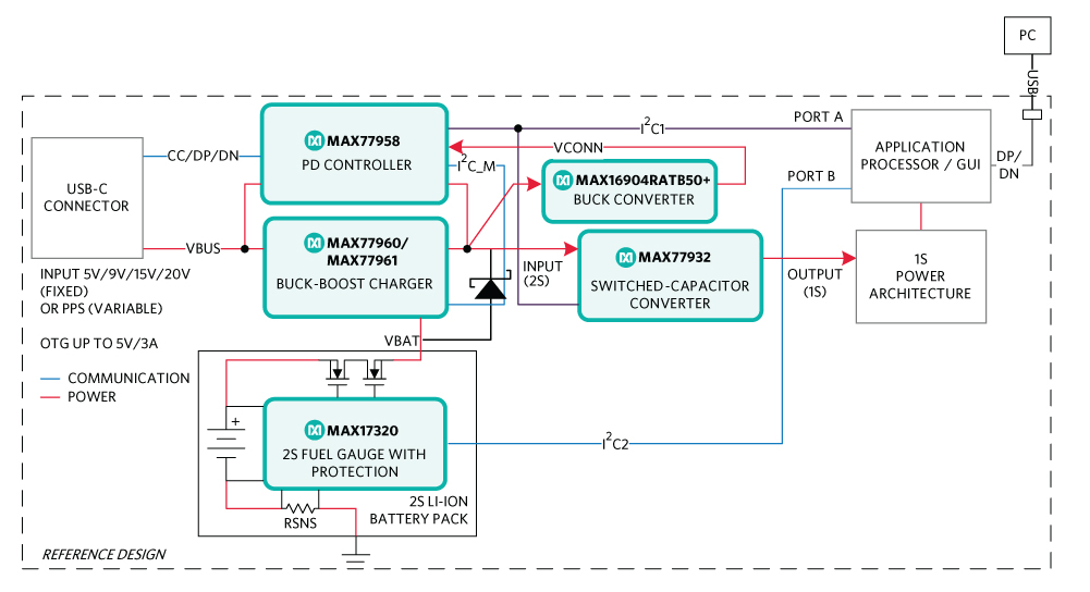
The MAXREFDES179 reference design board is a standalone 27W/45W USB type-C PD fast-charger, fuel-gauge, and protection solution for 2S Li+ batteries. It also provides 8A output at a voltage of 1S very efficiently to power systems with power management integrated circuits (PMICs) designed for 1S voltages.
The MAXREFDES179 allows the easy evaluation of the USB-C PD controller, buck-boost charger, fuel gauge with integrated protection, and 2S-to-1S switched-capacitor converter.
The MAX77958 is a complete solution to detect the USB type-C CC and implement the PD protocol. The MAX77960/MAX77961 is a 27W/45W wide-input buck-boost charger with integrated field-effect transistors (FETs) for 2S Li+ batteries. The MAX77932 is a dual-phase switched-capacitor converter with integrated power switches that delivers 8A output current and divides the input voltage by two. The MAX77932 also simplifies the migration by converting the 2S battery voltage to 1S-equivalent output and preserves the existing downstream 1S power architecture. The MAX17320 is a fuel-gauge IC with a protector and SHA-256 authentication for two to four series lithium-ion/polymer batteries. The fuel gauge uses the ModelGauge m5 algorithm that automatically compensates for cell aging, temperature, and discharge rate, and provides accurate state-of-charge (SOC) in milliampere-hours (mAh) or percentage (%) over a wide range of operating conditions to protect the battery.
The graphical user interface (GUI) is Windows-based. A register-based interface exercises the features of the MAX77932, MAX77958, MAX77960/MAX77961, and MAX17320.
The design files, firmware, and software are available in the Design Resources tab. The board is also available for purchase.
Features & Benefits
Input operating range of 3.5V to 25V
Type-C and USB-PD support
DRP and Try,Snk state
Cable orientation, power role detection
Integrated VCONN switch with OCP
Autonegotiate for the highest PD power profile (45W) when Sink
Autoenable OTG when Source
Autoconfigurable battery charger
AP control to overwrite PD power profile, OTG limit, USB-PD functions, buck-boost charger configuration, read/write MAX17320 fuel gauge status, configure MAX77932 switched capacitor converter
The reference design board is fully assembled and tested. Follow the steps to verify the board operation:
Identify the connections and test points (Figure 1). Confirm all the shunts and jumpers are at their default positions (Table 1).
Install the MAXREFDES179 Battery Power and MAXREFDES179 Battery Fuel Gauge software (GUI) on the PC.
Connect the Micro-B USB cable from the PC to the MAXREFDES179 reference design board. The Light-Emitting Diodes (LEDs) light up. Figure 3 shows the driver is installed properly.
Set up the test circuit (Figure 4). Preset the battery simulator to 7.4V and current limit to 100mA.
Toggle SW2 to wake the MAX17320 fuel gauge (needed only to power cycle the board).
Ensure the battery sourcing current is low (<100mA). Then only increase the current limit to 5A.
Start the MAXREFDES179 Battery Power GUI and click Connect. A pop-up message indicates the successful connection (Figure 5). Proceed with Read and Close.
Start the MAXREFDES179 Battery Fuel Gauge GUI. It automatically connects to the reference design.
Read the status of the USBC, charger, 2S to 1S battery voltage conversion, and fuel gauge.
The reference design completes its initialization. The VBUS, VSYS, and I2C pull up. The CC pin waveforms can be monitored using the oscilloscope (Figure 13).
Figure 3. Safely remove hardware.
Figure 4. Quick start connection diagram.
Figure 5. MAXREFDES179 Battery Power GUI connection.
Contact the respective Maxim representative to download the GUI.
The Future Technology Devices International (FTDI) drivers installation guide is available on the FTDI webpage.
Switched-Capacitor Converter, Fuel Gauge, Charger, and USB-C Measurement Points
The reference design board has various test points to evaluate the performances of the switched-capacitor converter (MAX77932), fuel gauge (MAX17320), buck-boost charger (MAX77960/MAX77961), and USB-C PD (MAX77958). Table 2, Test points, summarizes the recommended test points.
Table 1. Default shunt positions and jumper descriptions (MAX77932, MAX17320, MAX77960, and MAX77958 configurations)
USB-C
Default Position
Function
J9
Pin 1-2
VCIN supply to MAX77958
J32
Open
GPIO6 = pull down 330k to GND, MAX77958 slave address 0x27'h
J40
Open
GPIO6 = pull up 330k to VIO1, MAX77958 slave address 0x26'h
J41
Pin 1-2
GPIO6 = GND, MAX77958 slave address 0x25'h
J15
Pin 1-2
Connect VBUS to DCIN
J16
Pin 1-2
Connect SYS to MAX77958
J21
Pin 1-2
Connect MAX77958's SCL_M to MAX77960
J22
Pin 1-2
Connect MAX77958's SDA_M to MAX77960
J20
Pin 1-2
MAX77960's INTB to MAX77958's GPIO8
J19
Open
3.3V supply to VIO2
J33
Pin 1-2
1.8V supply to VIO2
J34
Pin 1-2
1.8V supply to VIO1
J35
Pin 1-3
MAX77958's GPIO2 to enable/disable VCIN supply
Charger
Default Position
Function
J5
Pin 2-3
OTG = I2C control
J3
Pin 2-3
QBAT = I2C control
J7
Pin 2-3
STBY = I2C control
J13
Pin 1-2
Connect THM to 10k thermistor pull down to GND to indicate battery is connected and temperature is normal.
Figure 15. Enable and disable MAX77932 by the EN pin.
Figure 16. Enable and disable MAX77932 by the I2C configuration.
Figure 17. Enable MAX77932 by the EN pin and disable MAX77932 by the VIO signal.
Figure 17. Enable MAX77932 by the EN pin and disable MAX77932 by the VIO signal.
Demo 2: Power Adapter is Connected When in Battery Mode
Figure 18 shows that the MAXREFDES179 reference design board setup supports autonegotiate for the highest PD power profile. Any USB-C PD adapter between 15W to 100W can be plugged in. The default highest PD power profile is 45W (15V/3A). Follow the steps to read the status:
Figure 19 shows the VBUS waveform when the power adapter is connected.
Read the USBC Status and observe the VBUS analog-to-digital converter (ADC) changes (Figure 20).
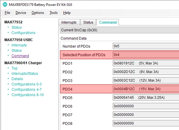
Read the current SrcCap, charger configuration, and status (Figure 21 and Figure 22).
Figure 23 shows the battery charging voltage and current.
Figure 18. Enable MAX77932 by the EN pin and disable MAX77932 by the VIO signal.
Figure 19. Autonegotiate for the highest PD power profile.
Figure 20. VBUS ADC status.
Figure 21. Current SrcCap (0x30) indicates negotiated PD power profile.
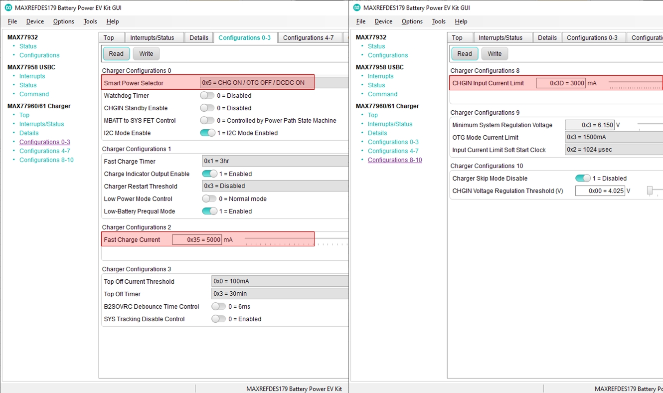
Figure 22. Charger configurations and details.
Figure 23. Battery charging voltage and current shown in the fuel gauge (MAX17320) GUI.
Demo 3: Manual Negotiation for a Different PD Profile
The MAXREFDES179 reference design board is user-programmable to negotiate for a different PD profile. Follow the steps to program to the other PD profile:
Battery Mode Setup - Plug in the USB-C PD power adapter (USB compliant) and connect the GUI (Figure 24).
Go to the Command tab → Select Current SrcCap (0x30) and click Write to read the selected PDO and current source capabilities of the far-end device. For example, the negotiated highest PD power profile is 15V, 3A (Figure 25). Fill the SrcCap request and click Write to request for a different source capability. For example, request for PDO2 (9V, 3A) as the new PD power profile (Figure 26).
The VBUS changes from 15V to 9V (Figure 27).
Read the newly selected PDO in the Current SrcCap (0x30) and USB status (Figure 28).
Figure 24. Manual negotiation for a different PD profile battery-mode setup.
Figure 25. USB-C command - current SrcCap before negotiating for a different PD profile.
Figure 26. USB-C command - SrcCap request for PDO2 (9V,3A).
Figure 27. VBUS changes from 15V to 9V.
Figure 28. Current SrcCap and USB-C status after a new PD power profile is established.
Demo 4: Sink (PPS) with GUI Control
The MAXREFDES179 reference design board is user-programmable to negotiate for a different PD profile. Follow the steps to program to the other PD profile:
Battery Mode Setup - Insert a 25W USB-C PD power adapter (PPS) and connect the GUI (Figure 29).
The AP has full control to achieve the best battery-charging efficiency by optimizing (increase/decrease) the VBUS voltage and current level.
MAXREFDES179 Battery Power GUI → Tools → Run Scripts → Select Scripts PPS_5V_to_11V_to_5V_2.25A → Execute. The scripts demonstrate that the PPS function is enabled and request a new APDO
(+500mV per second) from 5V to 11V. The scripts request a new APDO (-500mV per second) from 11V to 5V once the VBUS reaches 11V (Figure 30).
Figure 29. Insert the USB-C PD power adapter with the PPS features.
Figure 30. AP requests new VBUS level (500mV) every second to demonstrate the PPS features.
Demo 5: OTG Mode
The MAXREFDES179 reference design board supports the OTG mode autonomously. Follow the steps to read the OTG status:
OTG mode setup - Ensure the battery simulator is connected to the BATTP and BATTN pins. The GUI reads the register status. Plug in the OTG cable/device (Figure 31).
The VBUS is enabled during the OTG mode (Figure 32).
Read the USBC Status and observe the VBUS ADC (Figure 33).
Read the charger configuration (Figure 34 and Figure 35).
Figure 31. OTG mode setup.
Figure 32. VBUS during the OTG mode.
Figure 33. USB-C status is enabled during the OTG mode.
Figure 34. Smart power selector is enabled during the OTG mode.
Figure 35. Charger configuration is enabled during the OTG mode.
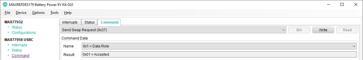
Demo 6: Initiate the Power Role Swap/Data Role Swap/VCONN Swap
The MAXREFDES179 reference design board is user-programmable to initiate the power role swap, data role swap, and VCONN swap. Connect to another MAXREFDES179 reference design board and follow the steps to initiate the power role swap:
Setup for the power role swap/data role swap/VCONN swap (Figure 36).
Go to the Command tab and select Send Swap Request (0x37). Select 0x2 = Power Role in the drop down and click Write (Figure 37).
The power role swap request is accepted (Figure 38).
VBUS transitions from the Source to Sink (Figure 39).
USB-C status after the power role swap is successful (Figure 40).
Figure 36. Setup for the power role swap_data role swap_VCONN swap.
Figure 37. Send swap request.
Figure 38. Initiate power role swap is successful.
Figure 39. VBUS transition from the source to sink after the power role swap.
Figure 40. USB-C status after the power role swap.
Follow the steps to initiate the data role swap:
Go to the Command tab → Select Send Swap Request (0x37). Select 0x1 = Data Role in the drop down and click Write. The data role swap request is accepted (Figure 41).
USB-C status after the data role swap is successful (Figure 42).
Figure 41. Initiate data role swap is successful.
Figure 42. Initiate data role swap is successful.
Follow the steps to initiate the VCONNswap:
Go to the Command tab → Select Send Swap Request (0x37). Select 0x3 = VCONN in the drop down and click Write. The VCONN swap request is accepted (Figure 43).
VCONN transitions from on to off (Figure 44).
USB-C status after the VCONN swap is successful (Figure 45).
Figure 43. Initiate VCONN swap is successful.
Figure 44. VCONN transition from on to off.
Figure 45. USB-C status after the VCONN swap..
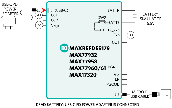
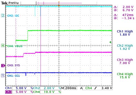
Demo 7: Dead-Battery Bootup
The MAXREFDES179 reference design board supports the dead-battery bootup. Plug in any USB-C PD adapter between 15W to 100W. The default highest PD power profile is 45W (15V/3A). Follow the steps to read the USB-C and charger statuses after the dead-battery bootup:
Dead-battery setup – Supply the BATT+ and BATT- pins with 5.5V (the battery is fully depleted when the battery drops below 5.6V). Plug in a USB-C PD power adapter (preferably USB-compliant). Connect the GUI to the reference design (Figure 46).
VBUS during dead-battery bootup (Figure 47).
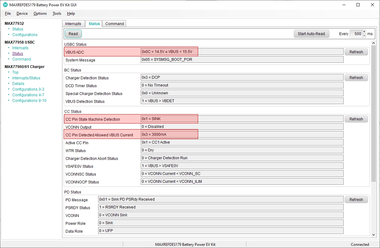
Read the USBC Status and observe the VBUS ADC (Figure 48).
Go to the Command tab → Select Current SrcCap (0x30) and click Write to read the selected PDO and current source capabilities of the far-end device (Figure 49).
Read the charger status and configurations (Figure 50 and Figure 51).
Figure 46. Dead-battery setup.
Figure 47. VBUS during the dead-battery bootup.
Figure 48. USB-C status after the dead-battery bootup.
Figure 49. Current SrcCap for the dead-battery bootup.
Figure 50. Charger details during the dead-battery bootup.
Figure 51. Charger configurations during the dead-battery bootup.
Search our knowledge base for answers to your technical questions. Our dedicated team of Applications Engineers are also available to answer your technical questions.