CN0568


Overview
Design Resources
Design & Integration File
- Schematic
- Bill of Materials
- Gerber Files
- Assembly Drawing
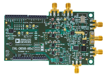
Evaluation Hardware
Part Numbers with "Z" indicate RoHS Compliance. Boards checked are needed to evaluate this circuit.
- EVAL-CN0568-ARD1Z ($428.00) 8.3GHz to 15.1GHz PLL and Quadband VCO
- EVAL-CN0568-ARD2Z ($428.00) 11.9GHz to 18.3GHz PLL and Quadband VCO
- EVAL-CN0568-ARD3Z ($481.50) 18.1GHz to 24GHz PLL and Quadband VCO
- EVAL-SDP-CK1Z ($160.00) System Demonstration Platform
Features & Benefits
- 8GHz - 26GHz Frequency Operation
- Quadband VCO provides Low Phase Noise over Wideband
- Onboard Reference Clock for ease of Use
- Arduino Form Factor Compatible
Documentation & Resources

Circuit Function & Benefits
Phase locked-loop (PLL) frequency generation circuits are ubiquitous across multiple industries and applications including basic FM broadcast band receivers, digital communications, aerospace, instrumentation, RADAR, and electronic warfare. PLLs are used to generate radio frequency (RF) and intermediate frequency (IF) signals from less than 1MHz to tens of GHz and higher. Application requirements vary widely, and PLL design and optimization involves trading off parameters such as power consumption, phase noise, frequency tuning range, frequency resolution, and lock time.
An important design tradeoff which must be considered that often results in undesirable performance compromises is that of frequency range versus phase noise performance. Wideband voltage con-trolled oscillators (VCOs) offer wide frequency range at the expense of optimal phase noise performance. In contrast, narrowband VCOs provide improved phase noise at the expense of tuning range achievable. It is possible to multiplex several narrowband VCOs to achieve a wider tuning range, but this is often not practical – complicated external circuitry is required to switch power to individual VCOs and select the appropriate RF output.
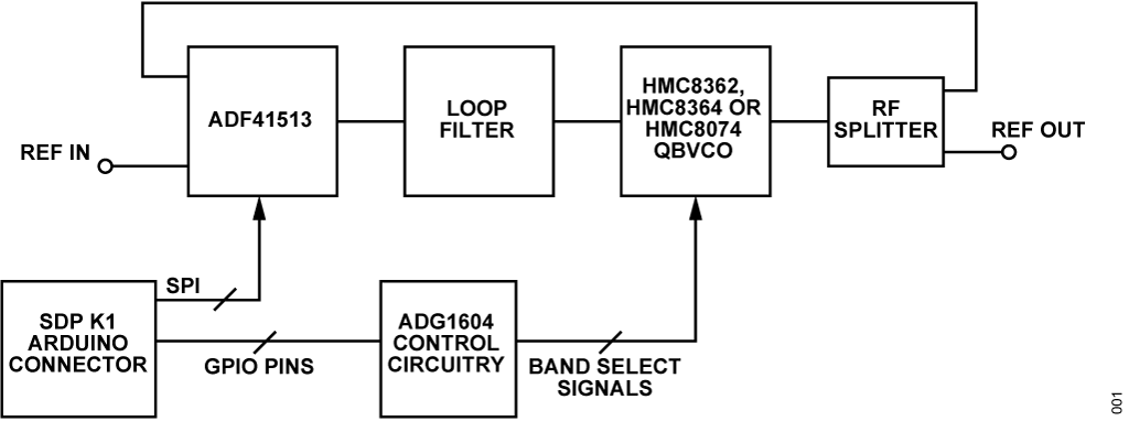
The circuit shown in Figure 1 features an integrated quadband VCO comprised of four narrowband VCOs within a single package. The advantage of this design is that it maintains the benefit of the excellent phase noise of a narrowband VCO, while also providing a wide frequency range of operation. VCO bands are switched through on-board multiplexer circuitry which selects from one of four VCOs based on the frequency programmed from the host.
This switching circuitry is optimized to provide ultra fast VCO band switching, which reduces overall lock time from frequencies in the lowest band through to the highest band. This is advantageous for applications that require fast switching time across a wide range of frequencies, such as fast frequency hopping.
The phase re-sync and phase adjust features included in the PLL are useful for applications such as beamforming, that requires highly accurate phase reproducibility. The circuit is compatible with Arduino form factor platform boards, and multiple boards can be stacked, sharing the same digital interface.

Circuit Description
PLL Synthesizer
The ADF41513 was selected as the PLL synthesizer for this circuit for its ultra-wide operating frequency range of 1GHz to 26.5GHz, which covers the entire frequency range of the 3 variants of quadband VCO. In fractional mode, the ∑-Δ modulator provides sub-hertz frequency resolution. The ADF41513 also has ultra-low noise floor performance -235 dBc/Hz in integer mode and -231 dBc/Hz in fractional mode for optimal phase noise performance.
Reference Input
The EVAL-CN0568-ARDxZ can be configured for an externally applied reference frequency from the REFIN SMA connector, or for the on-board ultra-low phase noise 100MHz crystal oscillator. This features an ultra-low jitter of 82fs jitter and close in phase noise of -90 dBC/Hz. By default, the board is configured for the on-board crystal oscillator option; the external input is selected by removing R8 and inserting a 0 Ω resistor in the R28 footprint. The onboard reference is recommended for any use cases where a 100MHz reference is required.
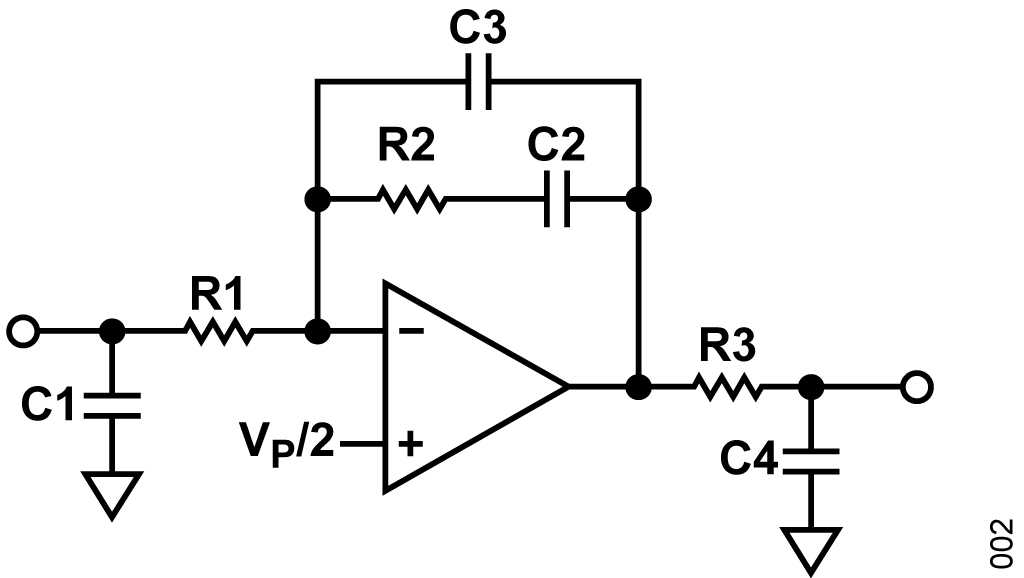
Loop Filter
The 1.0V to 13.5V tuning voltage requirements of the 3 variants of quadband VCO requires an active loop filter circuit with gain, as the charge pump of the ADF41513 PLL operates from 0 to 3.3v. The loop filter has been designed for maximum stability across the frequency range of each VCO band with an approximate loop band-width of 100kHz and phase margin of 50°. As the tuning sensitivity (frequency vs. tuning voltage slope) changes across the VCO band selected, the loop filter bandwidth will vary slightly depending on the frequency of operation. Since the loop filter has been designed for use with a 100 MHz reference frequency, it will need to be redesigned if any other reference frequency were required. The ADISimPLL tool can be used to determine the most suitable loop filter topology and to calculate the necessary component values for the desired bandwidth and phase margin using the simulation models.
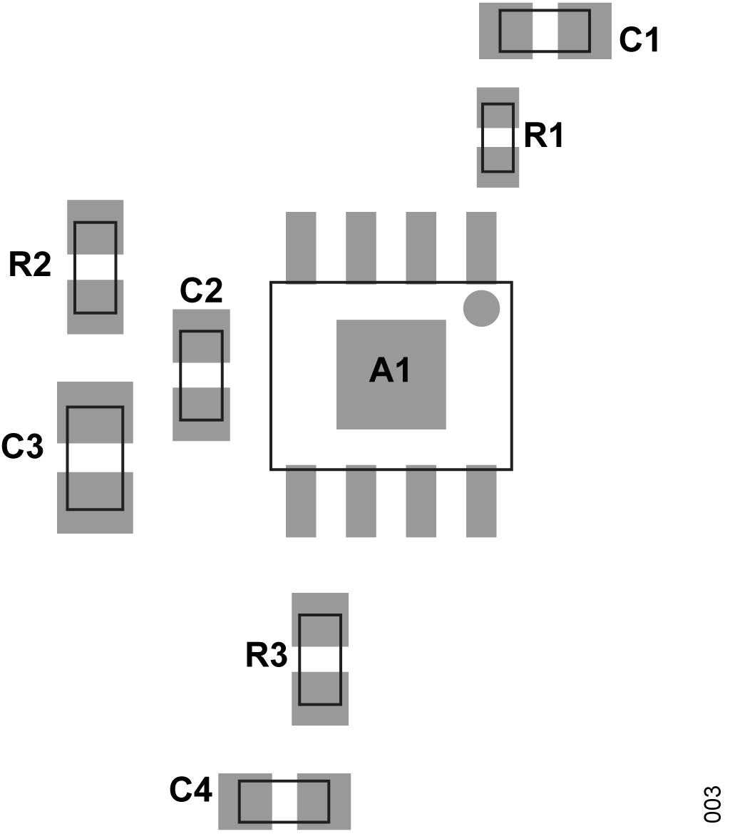
A fifth order loop filter topology was used for its increased out of band roll off and better attenuation of sigma delta modulator noise and spurs. The operational amplifier chosen for the loop filter was the ADA4625 which has low noise performance and can operate from rail to rail. Figure 2 shows a diagram of the loop filter configuration used. Figure 3 shows the footprint of the loop filter on the board.


Phase locked-loop (PLL) frequency generation circuits are ubiquitous across multiple industries and applications including basic FM broadcast band receivers, digital communications, aerospace, instrumentation, RADAR, and electronic warfare. PLLs are used to generate radio frequency (RF) and intermediate frequency (IF) signals from less than 1MHz to tens of GHz and higher. Application requirements vary widely, and PLL design and optimization involves trading off parameters such as power consumption, phase noise, frequency tuning range, frequency resolution, and lock time.
An important design tradeoff which must be considered that often results in undesirable performance compromises is that of frequency range versus phase noise performance. Wideband voltage con-trolled oscillators (VCOs) offer wide frequency range at the expense of optimal phase noise performance. In contrast, narrowband VCOs provide improved phase noise at the expense of tuning range achievable. It is possible to multiplex several narrowband VCOs to achieve a wider tuning range, but this is often not practical – complicated external circuitry is required to switch power to individual VCOs and select the appropriate RF output.
The circuit shown in Figure 1 features an integrated quadband VCO comprised of four narrowband VCOs within a single package. The advantage of this design is that it maintains the benefit of the excellent phase noise of a narrowband VCO, while also providing a wide frequency range of operation. VCO bands are switched through on-board multiplexer circuitry which selects from one of four VCOs based on the frequency programmed from the host.
This switching circuitry is optimized to provide ultra fast VCO band switching, which reduces overall lock time from frequencies in the lowest band through to the highest band. This is advantageous for applications that require fast switching time across a wide range of frequencies, such as fast frequency hopping.
The phase re-sync and phase adjust features included in the PLL are useful for applications such as beamforming, that requires highly accurate phase reproducibility. The circuit is compatible with Arduino form factor platform boards, and multiple boards can be stacked, sharing the same digital interface.
Voltage Controlled Oscillator
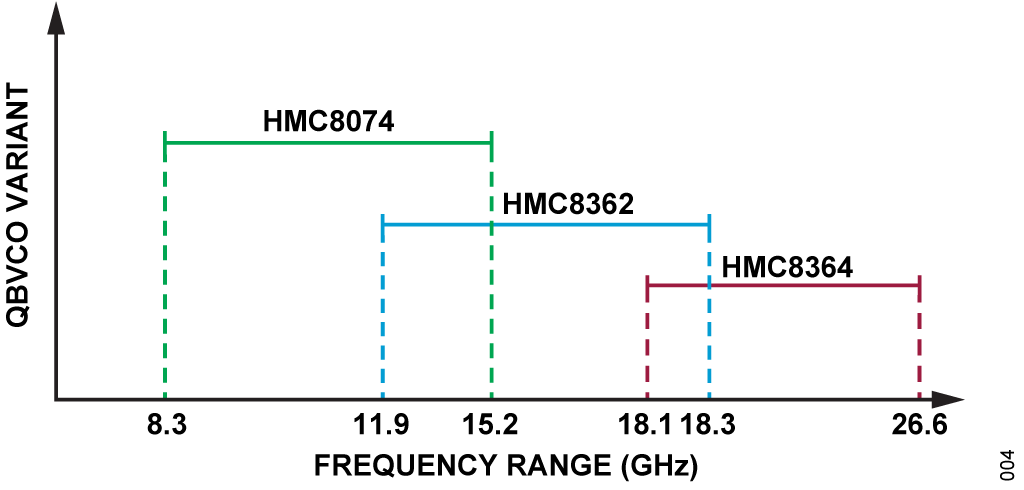
The HMC8074/HMC8362/HMC8364 quadband VCOs each consist of 4 independent narrowband VCO cores integrated into a single LFCSP package. Each core is selectable by applying a 5v supply voltage for the corresponding core. Only one core can be powered up at any given time to ensure that the output buffer amplifier is not overdriven. These quadband VCOs have the frequency range of a wideband VCO while maintaining excellent phase noise performance due to the narrowband performance of each internal VCO core. The VCO tuning curve remains consistent throughout all 4 frequency bands for a given part variant, allowing a single loop filter to be used for all bands. These quadband VCOs also offer a low typical current consumption of 75mA, including the buffer amplifier, for power sensitive applications. Together the three variants of quadband VCO cover a range of frequencies from 8.3GHz to 26.6GHz. The individual frequency ranges of each quadband VCO are as follows:
- HMC8074: 8.3 GHz to 15.2 GHz
- HMC8362: 11.9 GHz to 18.3 GHz
- HMC8364: 18.1 GHz to 26.6 GHz

Although the HMC8364 has the capability of operating up to the ADF41513 maximum frequency of 26.5GHz, the EVAL-CN0568-ARDxZ is limited to a 24GHz operating range. This is described in more detail in the Frequency Sensitivity section.
RF Splitter
An ultra-wide bandwidth (1.8-28GHz), 1:2 RF splitter splits the VCO output to the CN0568 RF output port and the PLL RF feedback path. This splitter was chosen primarily because of its wide band-width of 2GHz to 26.5GHz operating range. This means that the splitter can be used across the frequency range of all three variants of quadband VCO. The EP2K1+ also has high power handling capability of 2.5W in a small footprint of 4 4mm.


The insertion loss varies over the frequency range of the splitter from a typical 0.8dB at 2GHz to 2.4dB at 26.5GHz. This insertion loss must be added to the splitter loss of 3dB to provide the total loss that a signal experiences through the splitter at a certain frequency. At higher operating frequencies on the HMC8364 variant board, the insertion loss can affect locking as the RF input sensitivity of the ADF41513 increases with frequency. This is described in more detail in the Frequency Sensitivity section.
Phase Resync
When locking to a desired frequency, the phase can settle to any phase offset with respect to the reference frequency. Phase resync is a feature of the ADF41513 that produces a consistent phase offset from the reference, for a given RFOUT frequency. This is an important feature is phase-critical applications such as beamforming.
After first enabling phase resync the user then selects a phase offset at the frequency of operation. If the frequency is changed and then subsequently changed back to the original frequency, the original phase offset is maintained. When phase resync is enabled, an internal timer generates sync signals at intervals of tSYNC given by the following formula:
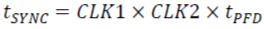
CLK1 and CLK2 are ADF41513 register bitfields that are program-med within the applications software. They must be programmed such that tSYNC is greater than the worst case lock time of the PLL to ensure that phase resync occurs on the last cycle slip of the PLL settling transient. Note that if Phase Resync is used, the sigma delta modulator must also be enabled, even if operating in integer mode.
Phase Adjust
The phase can be manually incremented at any given frequency using the phase value bitfield, which is programmed within the CN-0568 applications software. The phase offset is produced by using the following formula:
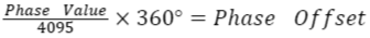
The phase can then be incremented by the phase offset amount each time register 0 of the ADF41513 is written to. As is the case with phase resync mode, the sigma-delta modulator must be enabled to perform a phase adjust, even when operating in integer mode.
Frequency Sensitivity
The ADF41513 has a maximum input frequency of 26.5 GHz and the HMC8364 quadband VCO variant just above this at 26.6 GHz. However, as frequency approaches 24GHz, there are a number of factors, as outlined in this section, that can affect performance and cause the loop not to lock. Therefore, the circuit is only specified for a maximum operating frequency of 24 GHz. 24GHz is specified while operating at room temperature. However maximum operating frequency may reduce if temperature is elevated.
The first factor that affects locking is that the HMC8364 VCO output power reduces with increasing frequency in band 4. This is illustrated by the plot shown in Figure 6.

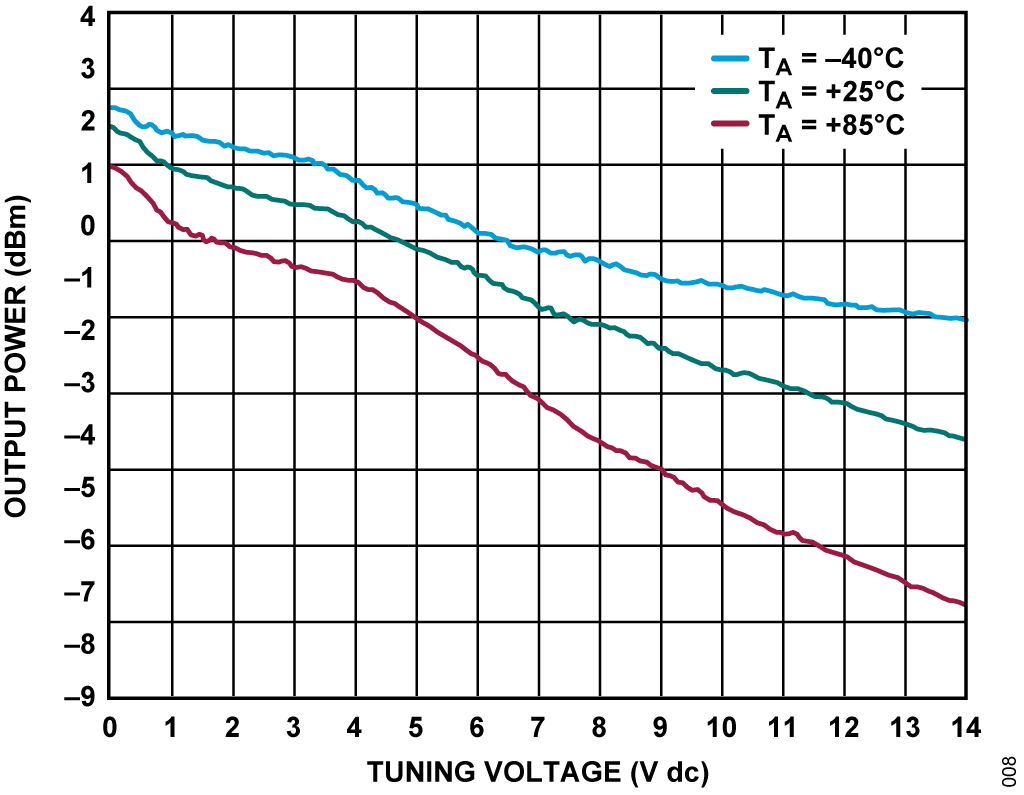
This reduced output power has a large contribution to the overall power loss in the circuit. A reduction in output power of up 6 dB can be seen between 23.9 GHz and 26.6 GHz.
The RF power splitter insertion loss also increases with frequency. This can produce up to an additional 1dB of loss at higher operating frequencies which contributes to the overall loss in the feedback loop.
Additionally, the RFIN frequency sensitivity of the ADF41513 in-creases with operating frequency. Above 24 GHz operating frequency, this sensitivity becomes more critical to operation as it is more difficult to meet the required output power due to the other loss contributors mentioned. The RF feedback traces can be redesigned for lower insertion loss at higher frequencies for a narrower frequency range. However, one of the objectives of this circuit is to demonstrate performance over the widest frequency range for all three variants of quadband VCO. Another technique to increase the power of the feedback signal is to add an amplifier in the feedback. This is outlined in the Common Variations section.
Control Circuit
The control circuit is used to select the different VCO bands based on the frequency selected in the applications software. GPIO signals are routed from the SDP-K1 Arduino connector to select a band based on the desired frequency. Custom firmware has been written for these GPIO control logic signals, which is provided on the CN0568 product page. See the Circuit Evaluation and Test section for details on loading the custom firmware.
One of the main components of the Voltage Controlled Oscillator band select circuitry is the ADG1604 4:1 multiplexer. This feeds a+5v supply voltage from a LT3045 regulator through one of the four switches of the multiplexer to the corresponding VCO band power supply. Using a multiplexer in the control circuit ensures that only one VCO core is powered up at a time, avoiding damage to the CO part. All control signals include filtering inductors and capacitors to attenuate noise and interference that may occur. Figure 7 is a simplified diagram of the control circuit for illustration purposes. (The complete schematic of the board including the control circuit is included in the CN0568 Design Support Package.)


The VCO integrated output buffer is powered up and down through a single pole double throw (SPDT) switch, which is controlled through another SDP-K1 GPIO signal. By default, this signal re-mains high after connection is established from the applications software.
Frequency Update Sequence
The frequency control registers on the ADF41513 are double buffered. This means that in order to change the RF output frequency, two events must occur. First the frequency control word registers must be updated according to the new desired frequency. Then a write to register 0 must be performed in order start the frequency change. A total of 4 registers, including the register 0 write, are writ-ten each time a frequency is updated on the applications software front panel. These registers must be written in the following order: Register 6, register 3, register 1 then register 0.
When a frequency is updated that uses a different VCO band to the current frequency, the GPIO control signals are updated after the register writes as illustrated in Figure 8.

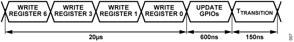
The GPIOs are updated approximately 600ns after register 0 is updated. The transition time is the delay time between the GPIO address bits changing and the corresponding output switch being multiplexed. The ADG1604 4:1 multiplexer has a transition time of typically 150ns.
Power Supply Regulation
The EVAL-CN0568-ARDxZ is powered by two external power supplies which are applied to on board SMA connectors. +25v is applied to V+SMA and 6v applied to J1. ADF41513 power supplies are grouped as per the default power supply grouping on the EV-ADF41513SDxZ evaluation board. Reducing the number of regulators by combining more power supply pins can produce undesired spurs appearing in the output frequency spectrum.
The +6v supply applied to J1 provides the input voltage for four on-board LT3045 LDO regulators. The LT3045 regulators were selected for their ultra-low noise performance and 500mA output current capability.
These regulators supply power to all +3.3V ADF41513 supplies as well as the +5v supply to the quadband VCO and crystal oscillator reference. The output voltage is configured on each regulator by setting the RSET resistor at the SET pin accordingly. See the LT3045 datasheet for more details.
The +25v supply is applied directly to the active loop filter supply from the external supply through the V+SMA. Decoupling capacitors are included in the supply path to mitigate against external noise degrading the supply.
Common Variations
To compensate for the reduction in output power above 24GHz on the HMC8364 quadband VCO variant, an amplifier can be included after the RFOUT signal. The amplified signal can then be used as the feedback signal to the RFIN port of the ADF41513 to increase the operating range to the maximum frequency of 26.5GHz. In Figure 9, a phase noise result was gathered connecting the HMC962 LNA to the RFOUT port. For comparison, this is then overlaid with the default configuration without the LNA.


As can be seen in Figure 9, there is no phase noise degradation when the HMC962 is included on the output. At 24 GHz, the gain of the amplifier is approximately 12.5 dB. In this case, the power level was -7.4 dBm input to the amplifier. A power level of 5.23 dBm was measured on the output. This is an ideally suited power level as it within the maximum and minimum sensitivity levels of the ADF41513 at 24GHz. For more information on the ADF41513 sensitivity levels refer to the data sheet.
Circuit Evaluation & Test
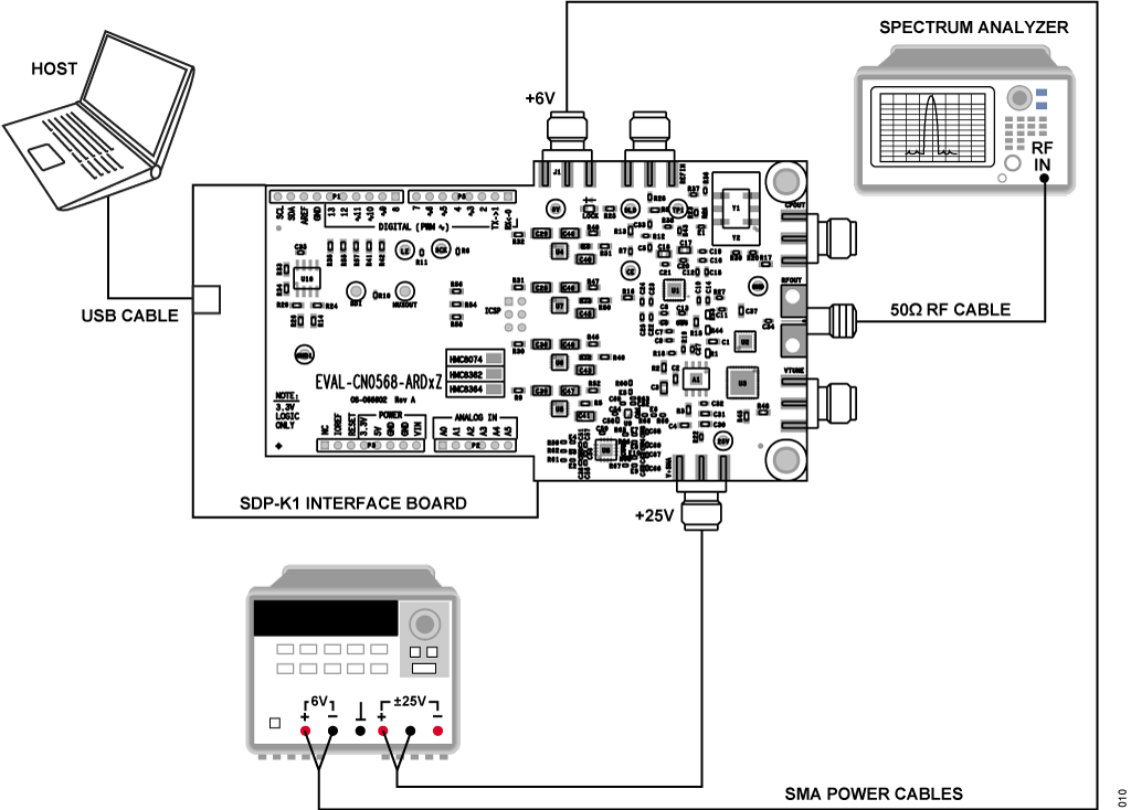
The EVAL-CN0568-ARDxZ board is interfaced to the host via an SDP-K1 controller board running CN0568-specific firmware. Other Arduino-compatible interface boards with 3.3v logic may be used but will require firmware development. The custom firmware file provided in the demonstration software installation is loaded into the SDP-K1 controller board after connecting for the first time. This is done by copying the hex file included in the software package to the SDP-K1 drive location.
Equipment Needed
- EVAL-CN0568-ARDxZ Evaluation Board
- EVAL-SDP-CK1Z controller board
- PC/laptop running windows 7 or later
- Spectrum Analyzer or Phase Noise Analyzer with suitable measurement frequency range
- 2 x Banana plug to SMA power cables
- 1 x 50 Ω RF / Microwave cable with 2.92mm connectors
- Dual power supply with +25v and +6v output voltage capability
Procedure
This section discusses the general procedure to setup the any variant of the EVAL-CN0568-ARDxZ to output a frequency on the RFOUT port. For more detailed instructions, consult the EVAL-CN0568-ARDxZ user guide.
- Ensure that power supplies are turned off. Set up the evaluation board as shown in Figure 10.
- Mount the EVAL-CN0568-ARDxZ to the SDP-K1 controller board.
- Connect host PC/laptop to the SDP-K1 interface board via a USB cable.
- Connect +6v (current limit = 200mA) to J1 and connect +25v (current limit = 20mA) to V+SMA.
- Connect the 50 Ω RF cable to the spectrum/phase noise analyzer.
- Turn on both power supplies.
- Open the CN0568 software and choose the correct variant. Then press ‘Connect’ button and initialize the part.
- Select a frequency within the operating range and select ‘Update Frequency’
- The frequency selected will then be visible in the spectrum analyzer.

Results
Phase noise results plots were gathered using the center frequency of the four bands of the HMC8362. Figure 11 shows the phase noise plots overlaid.

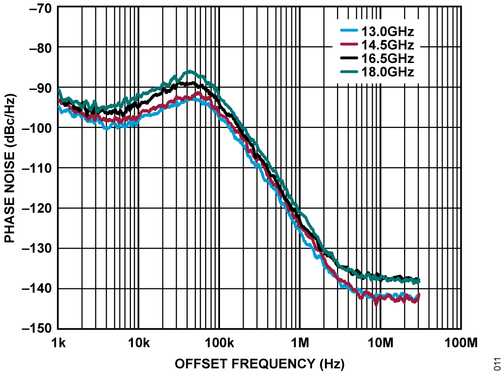
Results were gathered with the default on board loop filter configuration of 100kHz loop bandwidth, operating at room temperature. Measured lock times of the circuit are also presented for the EVAL-CN0568-ARD2Z in Table 1.
| Band Start/Stop | Start Freq. (GHz) | Stop Freq. (GHz) | Lock time (μs) |
| Band 1 - Band 2 | 13 | 14.5 | 53.1 |
| Band 1 - Band 3 | 13 | 16.5 | 28.5 |
| Band 1 - Band 4 | 13 | 18 | 49 |
| Band 2 - Band 1 | 14.5 | 13 | 55 |
| Band 2 - Band 3 | 14.5 | 16.5 | 56.7 |
| Band 2 - Band 4 | 14.5 | 18 | 36.5 |
| Band 3 - Band 1 | 16.5 | 13 | 35.8 |
| Band 3 - Band 2 | 16.5 | 14.5 | 54 |
| Band 3 - Band 4 | 16.5 | 18 | 57.1 |
| Band 4 - Band 1 | 18 | 13 | 47 |
| Band 4 - Band 2 | 18 | 14.5 | 32 |
| Band 4 - Band 3 | 18 | 16.5 | 50.2 |
For these lock times measured, the criteria for lock was that the frequency had reached +/- 10kHz of the stop frequency without subsequent deviation from his threshold. ADISimPLL has been used to verify simulated expected lock times are closely compara-ble to these measured results.