CN0507


Overview
Design Resources
Design & Integration File
- Schematic
- Bill of Materials
- Gerber Files
- Allegro Layout Files
- Assembly Drawing
- Eval Software
Evaluation Hardware
Part Numbers with "Z" indicate RoHS Compliance. Boards checked are needed to evaluate this circuit.
- EVAL-ADICUP3029 ($52.97) Ultra Low Power Arduino Form Factor Compatible Development Board
- EVAL-CN0507-ARDZ 2-Port Network Analyzer
Device Drivers
Software such as C code and/or FPGA code, used to communicate with component's digital interface.
Features & Benefits
- Complete 2-Port Vector Network Analyzer
- Frequency range from 1.7 GHz to 3.4 GHz
- Zero-IF System Architecture
Documentation & Resources
-
CN0507 User Guide4/16/2020WIKI
-
CN0507: User Guide (Rev. 0)4/10/2020PDF434 K
Circuit Function & Benefits
Vector network analysis is a technique to measure the phase shift and attenuation of signals as they propagate through a medium or are reflected by the medium. This technique is most commonly used to measure the gain, reflection coefficient, and reverse isolation of electronic circuits, such as RF amplifiers and filters, but can also be expanded to analyze characteristics of a material, such as its moisture content.
The reference design shown in Figure 1 implements a complete two-port radio frequency (RF) vector network analyzer using a zero intermediate frequency (ZIF) architecture. The frequency range of the circuit is from 1.7 GHz to 3.4 GHz, and the dynamic range is approximately 40 dB.
Directional couplers and in-phase-quadrature (IQ) demodulators sense the forward and reverse phase and amplitude. Because of the zero IF architecture, the IQ demodulator outputs are at dc and can be sampled directly by a precision analog-to-digital converter (ADC) integrated into a microcontroller.
A major advantage of the reference design is the use of the ZIF architecture, where use of a lower speed ADC reduces cost and avoids the design complexity associated with high speed sampling converters. This architecture enables the CN-0507 board to be compatible with low cost Arduino form factor boards and provides users with an alternative to bulky, expensive benchtop lab equipment that can cost thousands of dollars. The compact size of the reference design makes it ideal for a wide range of test and measurement applications.


Circuit Description
Analysis of a Linear Network
At RF, analysis of a linear network is executed using power waves, which can be related to the traveling voltage and current wave phasors. The scattering, or S-parameters, are the most common quantities to describe the electrical behavior of the network at high frequencies. The term, scattering, refers to the way the electromagnetic (EM) wave is affected as the wave passes a discontinuity.

Figure 2. S-Parameters
Figure 2 shows a two-port network with four traveling voltage wave phasors that are defined as follows:
- a1 is the incident wave at Port 1
- b1 is the reflected wave at Port 1
- a2 is the incident wave at Port 2
- b2 is the reflected wave at Port 2
- The four S-parameters of the network are defined as

A vector network analyzer measures the voltage wave phasors and computes the S-parameters.
Traditional Network Analyzer Architecture


Figure 3 shows the architecture of a traditional network analyzer, configured to measure dual-port S-parameters. Phase-Locked Loop 1 (PLL1) drives a sine wave into one of the two ports of the network, while the other port is internally terminated to 50 Ω. The device under test (DUT) or material under test (MUT) is generally connected between the RF ports (a MUT sample is placed between two antennae connected to the two ports).
While PLL1 conducts a stepped frequency sweep, portions of the incident, transmitted and reflected signals, are coupled off by four in-line directional couplers. These directional couplers drive four mixers that down convert the signals to a low intermediate frequency (IF). The local oscillator (LO) inputs of the four mixers are driven by a second PLL (PLL2).
For the intermediate frequency to remain constant, PLL1 and PLL2 need to track each other with a small offset frequency equal to the IF. This offset is usually a few hundred kHz. The circuit is completed by four IF sampling ADCs. The ADC outputs are digitally downconverted to baseband to yield amplitude and phase vectors. The S-parameters of the DUT or MUT are the ratios of these vectors.
With the absorptive single-pole double-throw (SPDT) switch in the position shown in Figure 3, PLL1 drives Port 1 and Port 1 is terminated to 50 Ω. With the amplifier under test connected as shown (input connected to Port 1), the sweep yields data that is used to calculate S11 (input reflection) and S21 (gain). By flipping the SPDT to its other position, PLL1 drives Port 2, yielding the data required to calculate S22 (output reflection) and S12 (reverse isolation).
Zero IF Architecture
An alternative approach is shown in Figure 4 in which the mixers are replaced with IQ demodulators and a single PLL is used to drive the DUT and the LO inputs of the IQ demodulators. This result yields baseband IQ vectors directly at the outputs of the IQ demodulators. Because the IQ demodulator outputs are at dc (while the PLL is at a particular frequency), the outputs be sampled by baseband ADCs (such as successive approximation (SAR) and low speed sigma delta (Σ-Δ architectures) rather than with IF sampling ADCs.


The ADF4355-3 PLL offers high output power, a wide frequency range, and dual outputs. In addition to providing the drive signal to the active port, the ADF4355-3 also provides LO drive for the four IQ demodulators.
The main signal path (starting at RFOUTA), as shown in Figure 5, consists of a programmable low-pass filter (HMC1044), a balun, two HMC8038 absorptive SPDT switches, and a bidirectional directional coupler
The HMC1044 filters the harmonics of the output signal of the PLL. The corner frequency of the HMC1044 must therefore be adjusted during the frequency sweep of the PLL. The first SPDT switch provides signal isolation during the dc offset calibration routine and the second SPDT switches the signal to either Port 1 or Port 2.
The bidirectional couplers have a coupling factor of approximately 15 dB and provide coupled forward and reverse signals to the four ADL5380 wideband IQ demodulators. The dc outputs of the four IQ demodulators are multiplexed down to a single pair of IQ signals by two ADG739 CMOS switches. Finally, these differential signals are applied to two AD8426 instrumentation amplifiers that convert the differential signals to single-ended signals with a dc offset of 1.25 V set by the ADR127 voltage reference. At this point, these two signals are routed to the standard analog input Arduino connector to be sampled by the integrated 12-bit ADC on the ADuCM3029.


The LO drive path (RFOUTB) also includes the HMC1044 programmable low-pass filter to reduce LO harmonics. This filter is followed by a balun, an HMC788A broadband gain block, and a passive 1-to-4 power splitter (built discretely on the board using resistors).
The availability of two synchronized but independent PLL outputs has multiple benefits. While the output power of the LO driving output (RFOUTB) is held steady, the output power level from RFOUTA (which drives the DUT or MUT) can be varied over a range of approximately 10 dB. This feature can be used to maximize dynamic range based on the application. For example, when measuring a passive device or material, the power level on RFOUTA can be set to its maximum. In contrast, when measuring an active device with gain, such as an RF amplifier, the PLL source power can be backed off so as not to overdrive the IQ demodulators.
IQ Demodulator DC Offset Compensation


To maximize dynamic range, the dc offset voltages at the outputs of the IQ demodulators must be measured and calibrated out.
The independent PLL outputs are used to full advantage during a dc offset nulling routine. Figure 6 shows the circuit and switch configuration during the dc offset nulling routine.
When the LO drive to the four IQ demodulators is turned on, the main signal path drive signal (RFOUTA) is turned off. To improve isolation, the first HMC8038 RF switch (the one which directly follows the HMC1044 low-pass filter) is configured so that its input is connected to the external 50 Ω resistor. The setting on the second HMC8038 RF switch depends on the port from which dc offset voltages are being measured.
When measuring the dc offset voltages of the IQ demodulators on Port 1, the second HMC8038 RF switch is configured so that its input is directed to Port 2. See Figure 7 for the proper configuration of the RF switches.


In this example, V1F, OFFSET (f) and V1R, OFFSET (f) are the measured forward and reverse voltages at Frequency f, respectively.
When measuring the dc offset voltages for Port 2, the second RF switch is toggled so that its input is now directed to Port 1. See Figure 8 for the proper configuration of the RF switches. Thus, V2F, OFFSET (f) and V2R, OFFSET (f) are the measured forward and reverse voltages at Frequency f, respectively
Note that the voltage measurements are complex. DC offset calibration for a single demodulator can be expressed as

where:
x is either Port 1 or Port 2.
y is either the forward or reverse voltage.
I and Q superscripts denote in-phase quadrature components.
Therefore, during dc offset calibration, eight offset voltages (an I and a Q offset voltage for each of the four IQ demodulators) are measured and stored. During all subsequent measurements, these voltages are subtracted before any data processing begins.


Short, Open, Load, and Through (SLOT) Calibration
Calibration is performed to improve the measurement accuracy of the vector network analyzer (VNA). In addition to correcting for impedance mismatch errors and signal leakage errors in the signal chain, calibration is also used to move the measurement reference plane to the desired location, thereby adjusting for phase shifts and insertion losses of cables and fixtures.
System calibration employs an error model that corrects the raw measured voltages. The error model includes a series of complex error coefficients that are calculated from measurements performed by applying known calibration standards (short, open, load, and through).
The 12-Term Error Model
The error model used in this example consists of 12 error coefficients or terms. This error model has separate forward and reverse signal flow graph models. In the succeeding discussion, s11, s12, s21, and s22 are the calibrated S-parameters of the DUT, whereas s11,M, s12,M, s21,M, and s22,M are the measured raw S-parameters. The two sets of S-parameters are related to one another using equations that contain the error terms calculated during calibration.
Figure 9 provides the forward flow graph error model and its six forward error coefficients:
- Directivity, e00
- Port 1 match, e11
- Reflection tracking, e10e01
- Transmission tracking, e10e32
- Port 2 match, e22
- Leakage, e30


To simplify the analysis of the graph model, scattering transfer parameters or T-parameter matrices are used. The T-parameter matrix can be defined and obtained from the S-parameters as

where Δs = s11s22 – s21s12.
Note that the Equation 1 definition already expresses the T-parameter matrix of the DUT.
When T1 is the T-parameter matrix for Port 1, the combined Port 1 and DUT flow graph is simply expressed as the matrix product, as follows:

The T-parameter matrix for Port 1 can be obtained as
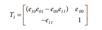
Because b2 = e22a2, the combined Port 1 and DUT system can now be simplified as

Expressions for b0 and a0 can easily be obtained from Equation 2. The measured reflection coefficient, S11,M, can then be expressed as

At Port 2,
b3 = e30a0 + e10e32b2
Diving by a0 yields the measured transmission coefficient s21,M

Figure 10 shows the reverse flow graph error model and its six reverse error coefficients:
- directivity e'33
- port 1 match e'11
- reflection tracking e'23e'32
- transmission tracking e'23e'01
- port 2 match e'22
- leakage e'03


Taking advantage of the symmetry between the forward and reverse flow graph, s22,M and s12,M can be expressed as

The calibrated S-parameters, s11, s12, s21, and s22 can be solved using the four equations of the measured raw S-parameters. Using linear algebra, it can be shown that

Performing Calibration and Calculating Error Terms
A standard calibration kit, consisting of short, open, and load elements is usually used during calibration. However, it is possible to use common terminations (for example, 50 Ω SMA termination for load, SMA short for short, and an open circuit for open) to calibrate and obtain reasonably accurate results in this frequency range.
The following are procedures and calculations that are required to apply to the 12 error coefficients of the model. Note that each calibration step yields different error terms.
Step 1: Reflection Calibration
The reflection calibration step involves measuring the reflection coefficient at each port using standard terminations. The standard terminations are short circuit (SC), open circuit (OC) and a fixed load (FL) of 50 Ω. The exact reflection coefficients of these standard terminations are assumed to be known (this data is generally provided with the calibration kit).


Figure 11 shows the flow graph of Port 1 with a standard termination. ΓCAL is the reflection coefficient of the termination. The combined Port 1 and standard termination flow graph can be represented by Equation 7.

The measured reflection coefficient ΓM at Port 1 can then be expressed as

Simplifying the equation yields
- e00 + ΓMΓCALe11 − ΓCALΔe = ΓM
With the three standard terminations, three equations are obtained, as follows:
- e00 + ΓM,OCΓCAL,OCe11 − ΓCAL,OCΔe = ΓM,OC
- e00 + ΓM,SCΓCAL,SCe11 − ΓCAL,SCΔe = ΓM,SC
- e00 + ΓM,FLΓCAL,FLe11 − ΓCAL,FLΔe = ΓM,FL
Next, solve the three error coefficients, e00, e11, and e10e01.
Figure 12 shows the flow graph of Port 2 with a standard termination.


Again, because of the symmetry between Port 1 and Port 2, the three equations using the three standard terminations are as follows:
e'33 + ΓM,OCΓCAL,OCe'22 − ΓCAL,OCΔ'e = ΓM,OC
e'33 + ΓM,SCΓCAL,SCe'22 − ΓCAL,OCΔ'e = ΓM,SC
e'33 + ΓM,FLΓCAL,FLe'22 − ΓCAL,FLΔ'e = ΓM,FL
where ΓM is the measured reflection coefficient at Port 2, and Δ'e = e'33e'22 − e'23 e'32.
Solve the next three error coefficients e'33, e'22, and e'32.
Step 2: Isolation Calibration
The isolation calibration step involves isolating the two ports by terminating both ports with a fixed load of 50 Ω, and then measuring the transmission coefficient. On the forward path, the forward leakage, e30, is just equal to the forward transmission coefficient, as shown in Equation 8.
e30 = s21,M
On the reverse path, the reverse leakage, e'03, is just the reverse transmission coefficient: e'03 = s12,M.
Step 3: Through Calibration
The through calibration step involves connecting the cables on the two ports together and measuring both the reflection and transmission coefficients. Note that, ideally the cables on Port 1 and Port 2 should have opposite genders to directly connect them together. If the two cables have the same gender, then a short SMA through should be used. This configuration, however, degrades overall accuracy, but results from lab measurements indicate that good accuracy is achievable if the through SMA element is relatively short.


Figure 13 shows the forward signal flow graph during a through calibration. The flow graph from Port 1 to the connecting planes of the two ports can be expressed as

The reflection coefficient at Port 1 can be obtained as

Note that the Port 2 match error coefficient, e22, is the only unknown in Equation 9. The error coefficients e00, e11, and Δe are obtained beforehand from the reflection calibration. Solving for e22

The signal at Port 2 can be written as;
b3 = e30a0 + e10e32ax
Diving by a0, yields s21,M

The forward transmission tracking error coefficient, e10e32, can now be obtained as
e10e32 = (s21,M – e30)(1 – e11e22)
Note that e11, e22, and e30 are known quantities at this point


Figure 14 shows the reverse signal flow graph during a through calibration. Because of the symmetry, the Port 1 match error coefficient, e'11, can be obtained as

Similarly, the reverse transmission tracking error coefficient, e'23e'01, can be derived as
e'23e'01 = (s12,M − e'03)(1 − e'11e'22)
Take note of the error coefficients obtained from the reflection and isolation calibrations.
Reflection Coefficients of Calibration Kit Short, Open, and Load Elements
Calibration kits generally provide the precise reflection coefficients of its short, open, and load elements. Less accurate but reasonable results can be achieved by using the ideal values shown in Table 1. These values can also be used if standard lab grade SMA connectors are used for calibration.
| Termination | Reflection Coefficient (ΓCAL) |
| Short | −1 |
| Open | +1 |
| Fixed 50 Ω Load | 0 |
A standard termination can be accurately modeled as a terminated transmission line, its signal flow graph is shown in Figure 15.


The transmission line is characterized by its reflection coefficient, ΓC, and propagation constant, γ.
The reflection coefficient, ΓL, is 0 for the 50 Ω load. However, the short and open terminations are modeled as inductive and capacitive loads, respectively. The inductor model for the short termination is a third-order function of frequency, as follows:
L(f) = L0 + L1f + L2f2 +L3f3
The load impedance of the short termination is then
ZL(f) = j2πfL(f)
The capacitor model for the open termination is also a third-order function of frequency
C(f) – C0 + C1f + C2f2 +C3f3
The load impedance of the open termination becomes
ZL(f) = 1/[j2πfC(f)]
From the load impedance, ZL(f), ΓL can then be obtained as
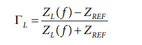
where ZREF = 50 Ω.
Using T-matrices, the terminated transmission line is characterized by the equation

where:

The matrix multiplication can be simplified as

The standard termination reflection coefficient, ΓCAL, can now be obtained as

The transmission line can also be characterized through its offset loss and offset delay, which are both easy to measure. The offset delay could also be obtained from termination length, l, as
Offset Delay = l/c
where c is the speed of light.
To account for the skin effect, the characteristic impedance, ZC, can be derived as

where Z0 is the lossless characteristics impedance of the transmission line, which is also 50 Ω. The propagation constant can also be expressed as
γl |= αl + βl
where:

If the offset loss is negligible and assumed to be 0, ΓCAL can be simplified as
ΓCAL = e−4πf(Offset Delay)ΓLΓCAL = 𝑒 -4𝜋f(offset delay) ΓL
Measured Results
Various measured results are shown in Figure 16, Figure 17, and Figure 18. To test the frequency range and dynamic range of the circuit, the Mini-Circuits® bandpass filter, ZAFBP-2100-S+ was used. Figure 16 shows the uncalibrated insertion loss and return loss of the filter. Figure 17 shows the response after calibration using a Keysight Technologies, Inc., 85033E standard mechanical calibration kit. Figure 18 shows the results of sweeps where 0 dB, −10 dB, −20 dB, −30 dB, and −40 dB attenuators are measured. All measurements use dc offset compensation.


Software Architecture
The 2-port vector network analyzer shield comes with two software components, as shown in Figure 19. The first software component is the firmware (right-hand side of Figure 19), which runs on the EVAL-ADICUP3029. The microcontroller unit (MCU) controls all the hardware devices of the network analyzer shield, such as the PLL, the multiplexing array, the programmable filters and the IQ demodulators. For each type of device, the firmware employs a device framework, which is a generalized model obtained by abstracting the function and behavior of a device. The firmware has been designed to have several layers of hardware abstraction in order to maintain modularity, enable code reuse and ease in code development and maintenance.
The second software component (left-hand side of Figure 19) is the computer application where the user can configure, calibrate, measure and view results. The application backend is responsible for processing all requests from the graphical user interface (GUI) as well as data handling. The computer application backend is also responsible for computing the s-parameters and performing calibration. For more specific details on the firmware and host application, see the CN0507 User Guide.


Firmware and Device Framework
Figure 20 shows the simplified block diagram of the 2-port network analyzer firmware. As shown in Figure 20, the MCU controls a single PLL, two multiplexing arrays, two low-pass filters, four I/Q demodulators, and two RF switches. The PLL, the multiplexing arrays, and the low-pass filters all share a single serial peripheral interface (SPI) bus.


Computer Application
The computer software component handles the calibration and the computation of the S-parameters. Figure 21 shows a screen capture of the application graphical user interface (GUI) that was developed using the open source platform of Node.js®. The GUI was designed to mimic bench type network analyzers.
All the settings and controls can be found on the right side of the GUI. Users configure the network analyzer with their desired sweep settings. Data handling between the computer application and firmware is optimized to produce an average sweep time of less than 1 second for a 100-point single-trace sweep, that is, processing a single S-parameter. Sweep time increases with the number of frequency points or steps and the number of S-parameters selected. To have a more consistent result, an averaging option is available. The GUI provides flexibility in viewing the results. Users have the option to select which S-parameters to plot, and whether to view the magnitude or phase of the S-parameters. As an additional feature, the plots of the S-parameters can be saved in S2P standard format.
Common Variations
The nominal frequency range of the circuit is 1.7 GHz to 3.4 GHz. This frequency range is largely determined by the Mini-Circuits BDCN-14-342+ directional couplers. By swapping out these directional couplers with pin-compatible alternatives listed in Table 2, the operating frequency can be reduced to as low as 360 MHz.
| Frequency Range | Recommended Part Number |
| 1.7 GHz to 3.4 GHz | BDCN-14-342+ (Mini-Circuits) |
| 0.824 GHz to 2.525 GHz | BDCN-15-25+ (Mini-Circuits) |
| 0.36 GHz to 1 GHz | BDCN-20-13+ (Mini-Circuits) |
The reference design provides an option to change the sensitivity of the network analyzer shield by varying the gain of the AD8426 instrumentation amplifier. Note that the dynamic range remains unchanged. An improvement in sensitivity is accompanied by a decrease in the compression point of the system.
In the original design, the gain setting resistors of the AD8426 have a value of 18.7 kΩ, which translates to an in-amp gain of 3.6× and a compression point slightly higher than 10 dB. By changing the resistors to 5.49 kΩ, the in-gain increases to 10×, but the compression point decreases to around 0 dBm. The effect of an in-amp gain of 10× on the sensitivity is shown in Figure 22.


Circuit Evaluation & Test
For evaluation and test, a standard 10 dB SMA attenuator can be used as the device under test (DUT). The attenuator, which is a common piece of laboratory equipment, is a useful DUT because of its obvious S-parameters (that is, S21 = S12 = −10 dB). The following is a list of equipment and software necessary to perform this circuit test.
Equipment Requirements
- The following equipment is required:
- EVAL-CN0507-ARDZ
- EVAL-ADICUP3029
- 6 V dc 2 A wall wart power supply
- 10 dB SMA attenuator
- Two short RF cables (SMA)
- PC with a USB port and Windows® 7 (32-bit) or higher
- USB type A to micro USB cable
Software Requirements
The following software is required:
- Analog Devices vector network analyzer computer application
- ADICUP3029 vector network analyzer firmware hex file
Test Setup Functional Block Diagram
A functional diagram of the test setup is shown in Figure 23.


Setup
Set up the circuit for evaluation as follows:
- Install the CN-0507 hardware on the ADICUP3029 platform board.
- Connect the CN-0507 to the 6 V dc wall wart power supply.
- Connect the EVAL-ADICUP3029 USB port to the PC.
a. An additional drive named DAPLINK appears on the PC. - Download the firmware to ADICUP3029 by dragging the ADICUP3029 vector network analyzer hex file into the DAPLINK drive. The drive disconnects and reconnects to indicate a completed download.
- Press the reset button of the ADICUP3029.
- Run the Analog Devices vector network analyzer computer application. Select the appropriate COM port and then select Connect. Leave the setting to its default.
- Leave the two ports of the network analyzer open. Click Start Sweep to perform a measurement.
- Hide S21 and S12. Figure 24 shows the measured S11 and S22. The ideal plot is a horizontal line at 0 dB.


Figure 24. Measured S11 and S22 with Ports Open and No Calibration - Unhide S21 and S12
- Hide S1 and S22.
- Connect the 10 dB SMA attenuator. Click Start Sweep to perform the measurement.
- Figure 25 shows the measured S21 and S12. The ideal plot is a horizontal line at −10 dB.


For an accurate measure, calibrate the vector network analyzer before performing measurement. For complete details of the operation of the hardware and software, read the CN-0507 user guide.