CN0418


Overview
Design Resources
Design & Integration File
- Schematic
- Bill of Materials
- Gerber Files
- PADS Files
- Assembly Drawing
Evaluation Hardware
Part Numbers with "Z" indicate RoHS Compliance. Boards checked are needed to evaluate this circuit.
- EVAL-ADICUP3029 ($52.97) ADuCM3029 Arduino Form Factor Compatible Development System
- EVAL-CN0418-ARDZ ($153.01) PLC Output Module with HART
Device Drivers
Software such as C code and/or FPGA code, used to communicate with component's digital interface.
AD5755 IIO Multi-Channel DAC GitHub Linux Driver Source Code
Features & Benefits
- 4-Channels
- +/- 10V , 4-20mA outputs
- HART Compatible
- Dynamic Power Control
- Digital Slew Rate Limiting
Markets and Technologies
Parts Used
Documentation & Resources
-
CN0418 User Guide7/23/2019WIKI
Circuit Function & Benefits
The circuit shown in Figure 1 provides a complete, fully isolated, and highly flexible, 4-channel analog output system suitable for industrial grade programmable logic controllers (PLCs), distributed control system (DCS), and other industrial process control applications that require ±5 V or ±10 V voltage and 4 mA to 20 mA current outputs with HART connectivity.
All 4-channel outputs and power input are protected from transient overvoltage and overcurrent events, suitable for the harshest industrial environments.
The CN0418 power entry circuitry includes on-board filtering and protection, and is compatible with supply voltages from 12 V dc to 36 V dc, including standard 24 V supplies common in many PLC and DCS applications.
The HART compatibility of this module provides a complete field communication solution that is simple to use, low cost, low power, and extremely reliable.
On-chip dynamic power control minimizes package power dissipation in current output mode, easing thermal management concerns in high channel count and high density applications where multiple circuits are used together.
Address selection logic allows up to four circuits to be stacked, providing up to 16 channels in a single node, maintaining isolation between banks of four outputs. An on-board electronically erasable programmable read only memory (EEPROM) can store calibration and identification data.


Circuit Description
Several standard voltage and current ranges are typically used in industrial control modules, including ±5 V, ±10 V, 0 V to 5 V, 0 V to 10 V, 4 mA to 20 mA, and 0 mA to 20 mA. The AD5755-1 provides all of these ranges at 16-bit resolution in a fully integrated, low cost, single-chip solution. A 20% overrange feature is also available for the voltage output ranges. Each DAC channel has a gain and offset register, which allow trimming of the gain and offset errors of the entire signal chain.
The current and voltage outputs are available on separate pins, but only one output type is active at a given time, thus allowing both output pins to be tied together and connected to a single terminal. When the current output is enabled, the voltage output is in tristate mode, and when the voltage output is enabled, the current output is in tristate mode. Analog outputs are short-circuit and open-circuit protected.
The AD5755-1 allows an internal or external precision, current setting resistor for the voltage to current conversion circuitry, as shown in Figure 2. The stability of the output current value over temperature is dependent on the stability of the value of the current setting resistor, RSET. As a method of improving the stability of the output current over temperature, an external 15 kΩ low drift resistor can be connected to the RSET_x pin of the AD5755-1 instead of the internal resistor. The external resistor is selected via the DAC control register. Accuracy measurements were evaluated using both options, as described in the Circuit Evaluation and Test section.


Precision Voltage Reference Selection
The AD5755-1 has an on-chip 10 ppm/°C (maximum) reference. For higher performance over temperature, this design uses an ADR02 reference with a 3 ppm/°C maximum drift (B grade, SOIC package). The voltage applied to the reference input provides a buffered reference for the DAC core. Therefore, any error in the voltage reference is reflected in the outputs.
The ADR02 is a 5 V precision reference that allows for an input voltage of up to 36 V. The ADR02 has a 0.06% maximum accuracy error and a 3 ppm/°C maximum temperature drift (B grade, SOIC package). This drift contributes approximately 0.02% error across the industrial temperature range of −40°C to +100°C.
The ADR02 has a long-term drift of 50 ppm (typical) and a 0.1 Hz to 10 Hz noise specification of 10 μV p-p (typical).
Dynamic Power Control
The AD5755-1 contains integrated dynamic power control using a dc-to-dc boost converter circuit, allowing reduced power consumption in the current output mode. Most PLC current output circuits use a fixed voltage source to meet the output voltage compliance requirements across the full range of load resistor values. For example, a 4 mA to 20 mA loop with 750 Ω load, when driving 20 mA, requires a compliance voltage of at least 15 V. However, when driving 20 mA into a 50 Ω load, only 1 V compliance is required. If the 15 V compliance is kept when driving the 50 Ω load, 20 mA × 14 V = 280 mW of power is dissipated as loss.
The AD5755-1 circuitry greatly reduces this power loss by sensing the output voltage and regulating the compliance voltage to allow only a small headroom voltage regardless of the load resistance. The AD5755-1 can drive up to 24 mA into a 1 kΩ load.
DC-to-DC Converter Operation
The AD5755-1 contains four independent dc-to-dc converters. These converters provide dynamic control of the VBOOST_x supply voltage for each channel. Figure 3 shows the discrete components external to the AD5755-1 associated with each channel.

Figure 3. DC-to-DC Circuit
Placing a 10 Ω, 100 nF low-pass RC filter after CDCDC is recommended. This filter consumes a small amount of power but reduces the amount of ripple on the VBOOST_x supply.
The dc-to-dc converters use a constant frequency, peak current mode control scheme to step up an AVCC input of 4.5 V to 5.5 V to drive the AD5755-1 output channel. These converters are designed to operate in discontinuous conduction mode (DCM) with a duty cycle of <90% typical.
When a channel is set to a current output range, the converter regulates the VBOOST_x supply to 7.4 V (±5%) or (IOUT_x × RLOAD + headroom), whichever is greater. In the current output mode with the output disabled, the converter regulates the VBOOST_x supply to 7.4 V (±5%). In voltage output mode with the output disabled, the converter regulates the VBOOST_x supply to 15 V (±5%). For full details of the dc-to-dc converter operation, see the AD5755-1 data sheet.
Digital Slew Rate Control
The slew rate control feature of the AD5755-1 allows the user to control the rate at which the output value changes. This feature is available on both the current and voltage outputs and serves two important functions: it reduces the transient current drawn from AVCC as an output is slewing from a low value to a high value, and it reduces disturbances to HART communication.
With the slew rate control feature disabled, the output value changes at a rate limited by the output drive circuitry and the attached load. With the slew rate feature enabled via the SREN bit of the slew rate control register, the output slews between two levels at a rate defined by the SR_CLOCK and SR_STEP parameters accessible via the slew rate control register.
The following equation describes the slew rate as a function of the step size, the update clock frequency, and the LSB size:
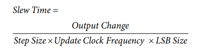
where:
Slew Time is expressed in seconds.
Output Change is expressed in amps for IOUT_x or volts for VOUT_x.
See the AD5755-1 data sheet for further details.
Transient Voltage Protection
The AD5755-1 contains ESD protection diodes that prevent damage from normal handling. However, the industrial control environment can subject input/output (I/O) circuits to much higher transients. To protect the AD5755-1 from excessively high voltage transients, a 24 V transient voltage suppressor (TVS) is placed on the IOUT_x/VOUT_x connection, as shown in Figure 4.


For added protection, clamping diodes are connected from the IOUT_x and VOUT_x pins to the VBOOST_x and AVSS power supply pins. A 5 kΩ current limiting resistor is also placed in series with the +VSENSE_x input. This resistor limits the current to an acceptable level during a transient event. The recommended external band-pass filter for the AD5700 HART modem includes a 150 kΩ resistor that limits the current to a sufficiently low level such that additional protection circuitry is not required, even in the most demanding industrial environments.
Input Power Protection
A regulated industrial standard supply, such as a 12 V dc or 24 V dc supply, is connected to the EVAL-CN0418-ARDZ board through a 2-wire or 3-wire interface. This supply must be protected against faults and electromagnetic interference (EMI) as shown in Figure 5.

Figure 5. Input Power Transient Voltage Protection
VR1, VR2, VR3, and VR4 are metal-oxide varistor surge suppressors, and F1 is a 1 A, resettable polyfuse. This circuit ensures that the reference design system survives interference and transients that may be present on the power ports. See PLC Evaluation Board Simplifies Design of Industrial Process Control Systems, Analog Dialogue 43-04, April 2009, for more details.
Power Supply Circuit
The EVAL-CN0418-ARDZ board is powered by a 12 V to 36 V dc supply and uses an on-board switching regulator to provide the 7.5 V supply to the platform board, as shown in Figure 6 and Figure 7. In the test setup, 7.5 V powers the EVAL-ADICUP3029 board. The EVAL-ADICUP3029 board then provides a regulated 3.3 V for the voltage at the IO_VREF pin (see Figure 7) and 5 V to the remaining circuitry.
The ADP2441 36 V step down, dc-to-dc regulator accepts an industrial standard 24 V supply, with wide tolerance on the input voltage. The ADP2441 steps the input voltage down to 7.5 V at 1 A for the platform board and 5 V power for the remainder of the EVAL-CN0418-ARDZ, utilizing the 5 V regulator typically present on Arduino-compatible platforms. The circuit also includes filtering and protection on the 24 V supply terminals.
The high switching frequency of the ADP2441 allows minimal output voltage ripple even when small inductors are used. Selecting the size of the inductor involves considering the tradeoff between efficiency and transient response. A smaller inductor results in larger inductor current ripple, which provides improved transient response but degrades efficiency. Due to the high switching frequency of the ADP2441, using shielded ferrite core inductors is recommended because of their low core losses and low EMI.
In the Figure 6 circuit, the switching frequency is approximately 550 kHz with the 162 kΩ external resistor. The inductor value of 33 μH is chosen from the ADP2441 data sheet. The circuit is connected to the field supply of 12 V to 36 V using screw terminals. The EARTH terminal can be connected to an external earth connection or to the GND terminal if an external earth connection is not used. Power inductors, varistors, a power diode, and a 1.1 A fuse provide additional input protection against high voltage transient events.
Isolated power is generated by an LT8301 no-opto isolated flyback converter. A transformer with a four-tap secondary winding provides isolation and generates +16 V, −16 V, and +5 V supplies. The output voltage is regulated by sampling the primary side flyback waveform, eliminating the need for opto-isolators, auxiliary sense windings, or other isolated feedback methods.
The LT8301 tends to regulate the most heavily loaded output in a multiple output circuit. The AD5755-1 presents a range of loading conditions to the +16 V supply, −16 V supply, and +5 V supply rails. Table 1 shows the supply voltages under various load conditions that meet the AD5755-1 requirements.


| Setup | +16 V Supply (V) | −16 V Supply (V) | +5 V Supply (V) |
| Power Circuit Unloaded, AD5755-1 Outputs Disabled | 16.15 | −16.15 | 4.8750 |
| AD5755-1 in Current Output Mode | |||
| 20 mA on Four Channels (1 kΩ Load) | 18.55 | −20.93 | 4.8936 |
| 24 mA on Four Channels (1 kΩ Load) | 19.64 | −22.11 | 4.8622 |
| AD5755-1 in Voltage Output Mode, 10 V on Four Channels (500 Ω Load) | 17.11 | −17.11 | 4.9476 |
The AD5755-1 has a wide supply voltage tolerance, but the circuit must be evaluated thoroughly when integrating to customer systems. Verify that the LT8301 maintains regulation of the isolated supplies within the allowable ranges listed in the AD5755-1 data sheet under all normal loading conditions, fault conditions, and over the expected range of input supply voltage.
HART Coupling
The AD5755-1 has four CHARTx pins, corresponding to each of the four output channels. A HART signal can be coupled into these pins and appears on the corresponding current output if that output is enabled. Table 2 shows the recommended input voltages for the HART signal at the CHARTx pin. If these voltages are used, the current output meets the HART amplitude specifications. Figure 8 shows the recommended circuit for attenuating and coupling the HART signals to the AD5755-1 HART inputs.
| RSET | CHARTx Input Voltage (mV p-p) | HART Current Output (mA p-p) |
| Internal RSET | 150 | 1 |
| External RSET | 170 | 1 |

Figure 8. Coupling HART Signal
A minimum capacitance of C1 + C2 is required to ensure that the 1.2 kHz and 2.2 kHz HART frequencies are not significantly attenuated at the output. The recommended values are C1 = 22 nF and C2 = 47 nF. Digitally controlling the slew rate of the output is necessary to meet the analog rate of change requirements for HART.
Digital Isolation
The ADuM3151 and ADuM3482 are 3.75 kV quad channel digital isolators in small 20-lead SSOP packages (7.2 mm × 7.8 mm). The isolator core operates between 3.0 V and 5.5 V, whereas the I/O supply can range from 1.8 V to 5.5 V. These devices can be used to interface directly with 1.8 V logic. The ADuM3151 in this design isolates the SPI signals for the AD5755-1 and GPIO controls to control the address lines of the ADG759 quad channel mux, while the ADUM3482 isolates the UART signals for the AD5700-1 HART modem. Stitching capacitance is implemented within the printed circuit board (PCB) itself by overlapping internal planes to reduce EMI radiation and board noise. For more information about EMI mitigation techniques, see the AN-0971 Application Note, Recommendations for Control of Radiated Emissions with isoPower Devices.
INL and DNL Performance
The integral nonlinearity (INL) of the AD5755-1 was tested using the transformer isolated switched power supply, as shown in Figure 9. The AD5755-1 data sheet specifies an INL of ±0.006% FSR across the full temperature range for both current output and voltage output, irrespective of whether the internal or an external RSET is used. Figure 9 and Figure 10 show that the measured results fall well within this specification.


Absolute Accuracy Performance
The specification for the total unadjusted error (TUE) for the AD5755-1 in current output mode using the internal RSET is ±0.11% FSR maximum at 25°C. The total error of the ADR02 reference (B grade) is 0.06% maximum at 25°C.
Table 3 shows the measured current output error of the circuit for Channel A in the 4 mA to 20 mA range with a 500 Ω load using the internal RSET. Table 3 summarizes the results for Channel A, using the internal RSET, but is indicative of all four channels. All results are within the expected values.
| Code | IOUT (mA) | Error (% FSR) |
| 0x0000 | 4.0002 | +0.0013 |
| 0x4000 | 7.9994 | −0.0038 |
| 0x8000 | 11.9988 | −0.0075 |
| 0xC000 | 15.9982 | −0.0112 |
| 0xFFFF | 19.9990 | −0.0063 |
Similar measurements were taken for the voltage output mode, where the AD5755-1 TUE specification is ±0.03% FSR maximum at 25°C. Table 4 shows the results for Channel A. The remaining three channels showed similar results.
| Code | VOUT (V) | Error (% FSR) |
| 0x0000 | −9.996915 | −0.000226 |
| 0x4000 | −8.776362 | −0.000179 |
| 0x8000 | −7.555827 | −0.000467 |
| 0xC000 | 5.001719 | 0.000766 |
| 0xFFFF | 10.001078 | 0.001526 |
HART Compliance
Figure 11 shows the 1200 Hz and 2200 Hz frequency shift keying (FSK) frequencies measured across a 500 Ω load resistor on IOUT_A. Channel 1 shows the modulated HART signal coupled into the AD5755-1 output (set to 4 mA), whereas Channel 2 shows the AD5700-1 TXD signal.


To be HART compliant, the circuit must meet the HART physical layer specifications. Numerous physical layer specifications are included in the HART specification documents. For evaluating the performance of the hardware, the two specifications considered in this circuit note are the output noise during silence and the analog rate of change.
Output Noise During Silence Test
When a HART device is not transmitting (silent), it does not couple noise onto the network in the HART extended frequency band. Excessive noise may interfere with reception of HART signals by the device itself or other devices on the network.
The voltage noise measured across a 500 Ω load must contain no more than 2.2 mV rms of combined broadband and correlated noise in the HART extended frequency band. Additionally, the noise must not exceed 138 mV rms outside of this frequency band.
This noise was measured by connecting the HCF_TOOL-31 filter (available from the HART Communication Foundation) across the 500 Ω load and subsequently connecting the output of the filter to a true rms meter. An oscilloscope was used to examine the output waveform.


Analog Rate of Change
This specification ensures that when a device regulates current, the maximum rate of change of analog current does not interfere with HART communications. Step changes in current disrupt HART signaling. The worst case change in the analog output current must not produce a disturbance higher than 15 mV peak, measured across a 500 Ω load in the HART extended frequency band. Meeting this requirement ensures that the maximum bandwidth of the analog signaling is within the specified dc to 25 Hz frequency band.
For this test, the HCF_TOOL-31 was again connected across the 500 Ω load, as in the noise during silence test, and an oscilloscope was connected to its output. Rather than setting the AD5755-1 output to a fixed output current, however, the AD5755-1 was programmed to output a cyclic waveform, switching from 4 mA to 20 mA. To meet the required system specifications, the output current change was limited by the digital slew rate control feature of the AD5755-1. This feature is described in more detail in the AD5755-1 data sheet. For this test, SR_CLOCK and SR_STEP were set to 64 kHz and 16 LSBs, respectively, giving a slew time of 64 ms. The result is shown in Figure 13. Channel 1 shows the AD5755-1 IOUT_A signal stepping between 4 mA and 20 mA, sensed across the 500 Ω load and connected to the input to the band-pass filter. The output of the filter (which has a gain factor of 10) can be seen on Channel 2. The peak value is within the previously mentioned 150 mV peak limits.


Common Variations
For applications requiring only current outputs, the AD5757 can be used as an alternative to the AD5755-1. If less than 16 bits of resolution is required, the 12-bit AD5737 can be used.
For applications that operate close to or at the maximum current of the AD5755-1, use the power solution shown in DC2906A demo manual (based on the LT8302), which provides higher output power.
The AD5700 modem can be used instead of the AD5700-1. However, either an external crystal or a CMOS clock is required because the AD5700 does not have the internal oscillator option provided on the AD5700-1. See the AD5700 data sheet and the AD5700-1 data sheet for further details.
For single channel applications, see Circuit Note CN0321, Fully Isolated, Single Channel Voltage and 4 mA to 20 mA Output with HART Connectivity.
Circuit Evaluation & Test
The provided software targets the EVAL-ADICUP3029 platform, but it is designed to be easily portable to other microcontroller platforms. When porting to other platforms, be sure to thoroughly review hardware compatibility, including voltage levels and functionality.


Required Equipment
The following equipment is required for operation:
- EVAL-CN0418-ARDZ reference design board
- Serial terminal program such as Tera Term or Putty
- EVAL-ADICUP3029 development board
- PC (Windows® 32-bit or 64-bit)
- 24 V power supply such as Agilent E3631A
- Precision voltage and current meter, such as Agilent 3458A
- Four 500 Ω precision load resistors
- Oscilloscope (Tektronix TDS2024B or equivalent)
- USB Type A to micro USB Type B
- CN0418 software
Getting Started
For more information and complete details on setup, reference the CN0418 user guide.
Software Installation
Follow these steps to install the software:
- Attach the EVAL-CN0418-ARDZ onto the EVAL-ADICUP3029 board.
- Connect the EVAL-ADICUP3029 board via the USB port of the PC using the supplied cable.
- Power up the EVAL-CN0418-ARDZ by applying 24 V to the terminal block P1 connector.
- Upload the firmware to the EVAL-ADICUP3029.
Functional Block Diagram
Figure 15 shows a functional block diagram of the test setup.


Follow these basic steps for setup:
1. Connect the EVAL-CN0418-ARDZ to the EVAL-ADICUP3029 as shown in Figure 16.


2. If the jumpers are not already mounted, mount the jumpers provided in the box in the same configuration as shown in Figure 17.
3. Apply 24 V dc to the P17 jumper of the EVAL-CN0418-ARDZ.
4. Connect the micro USB cable from the EVAL-ADICUP3029 to the PC.
5. Open a serial terminal window using a command line interrupter program such as Putty, Telnet, or Tera Term
For detailed instructions on how to set up the hardware and software to interface with the computer, reference the CN0418 user guide.