CN0535
High Performance, Alias Free Measurement Platform for Flexible Data Acquisition System


Overview
Design Resources
Design & Integration File
- Schematic
- Bill of Materials
- Gerber Files
- Assembly Drawing
Evaluation Hardware
Part Numbers with "Z" indicate RoHS Compliance. Boards checked are needed to evaluate this circuit.
- EVAL-CN0535-FMCZ ($176.55) High Performance, Alias Free Data Acquisition Board
- EVAL-SDP-CH1Z ($399.00) System Demonstration Platform
Device Drivers
Software such as C code and/or FPGA code, used to communicate with component's digital interface.
Features & Benefits
- Alias free Measurement System
- Optimized for AC & DC Performance
- Wide Analog Input (+/-12V)
- FMC Compatible Form Factor
Markets and Technologies
Parts Used
Documentation & Resources
-
CN-0535 User Guide2/3/2021WIKI
-
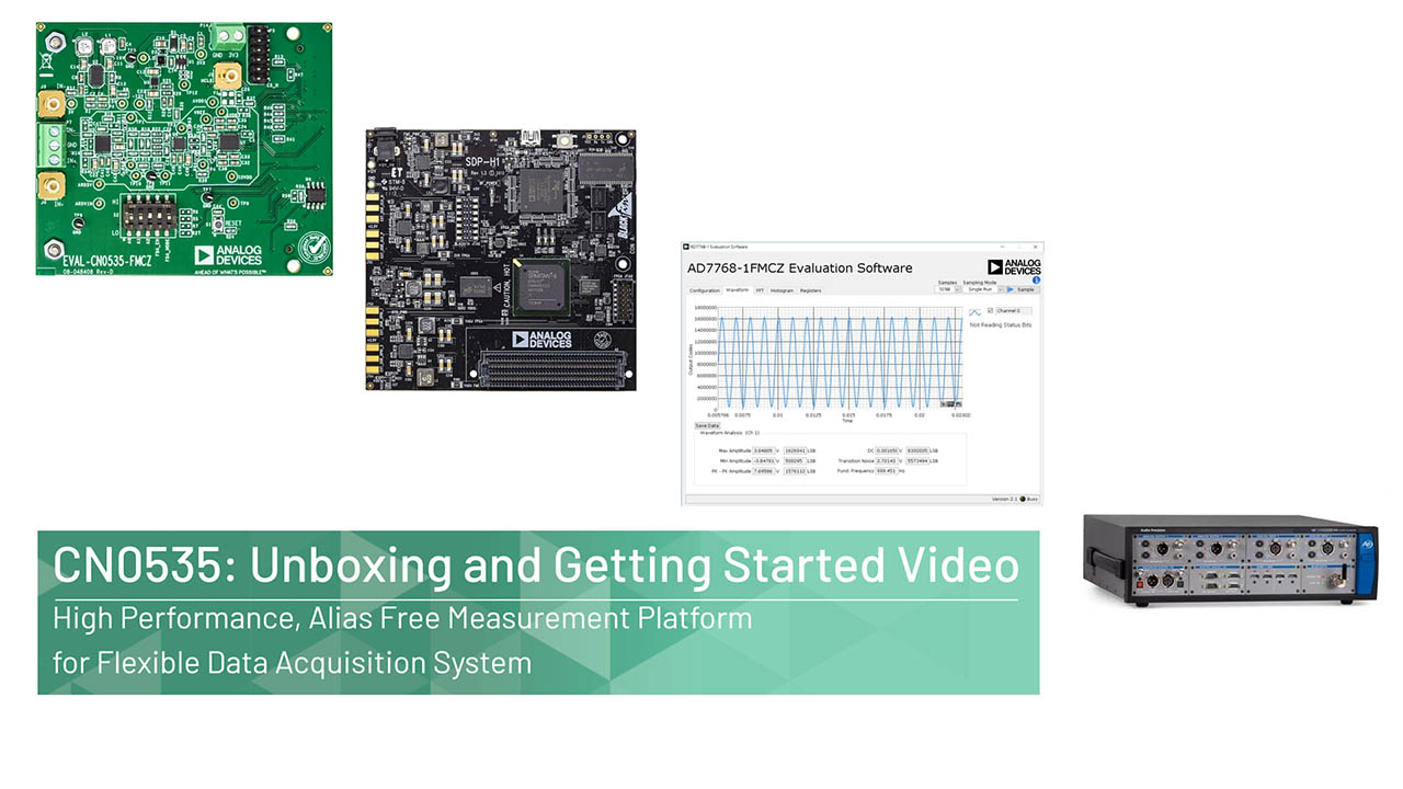 CN0535 Unboxing and Getting Started Video12/12/2024
 -
 CN0535 Mbed Example Program Setup12/12/2024

Circuit Function & Benefits
A data acquisition (DAQ) system measures real-world physical phenomenon, such as temperature, force, acceleration, or vibration, converting measurements into digital values for data processing, storage, or transmission to a remote location. A typical DAQ system is comprised of a sensor, analog filtering and signal conditioning circuitry, an analog-to-digital converter (ADC), and a digital controller. Components for a DAQ solution are selected on a per application basis. Some DAQ systems are designed to minimize the overall system dc error from the sensor, with fast settling filters for control loop or multiplexed applications. Others are designed to provide superior ac performance, with low distortion and flat frequency response.
The DAQ system shown in Figure 1 has simplified many of these design challenges into a single, flexible DAQ platform that can be used across a wide range of ac and dc applications.
The wide input voltage range, high input impedance, and high input common-mode voltage allows most sensors and signal sources to be connected directly to the input, without additional signal conditioning. The system has a programmable gain block for attenuation or amplification of the input signal to optimally utilize the input range of the ADC.
The dc and ac performance of this system have been optimized to provide exceptional performance across the entire analog input bandwidth. The low input bias current minimizes the dc error due to the output impedance of the sensor, and the high common-mode rejection ratio (CMRR) minimizes the impact of the common-mode noise pickup from the environment, especially when the sensor is located far from the DAQ system, which keeps the dc errors to a minimum, while not making sacrifices to the ac performance of the converter.
The ADC has fully programmable digital filters with adjustable bandwidth and data rate that can be tailor fit to specific system requirements. The analog filter of the system rejects frequencies at multiples of the sampling frequency, eliminating aliasing concerns.


Circuit Description
ADC
The heart of the solution is the AD7768-1, which is a low power, high performance, Σ-Δ ADC, with a Σ-Δ modulator and digital filter for precision conversion of both ac and dc signals. The AD7768-1 offers the user flexibility to configure and optimize for input bandwidth vs. output data rate (ODR) vs. power dissipation.
The ODR can be programmed on a per application requirement. Use the following equation to calculate the ODR of the AD7768-1:
ODR = (FMOD/DEC RATE)
where:
FMOD is the AD7768-1 modulator frequency.
DEC_RATE is the decimation rate.
Use the following equation to calculate FMOD:
FMOD = (MCLK/MCLK DIV)
where:
MCLK is the master clock frequency.
MCLK_DIV is the ratio between MCLK applied and the clock used by the ADC modulator.
The AD7768-1 offers extensive digital filtering capabilities that meet a wide range of system requirements. The filter options allow configuration for frequency domain measurements with tight gain error over frequency, linear phase response requirements (a wideband, low ripple, finite impulse response (FIR) filter), a low latency path (sinc5 or sinc3) for use in control loop applications, and measuring dc inputs with the ability to configure the sinc3 filter to reject a line frequency of either 50 Hz or 60 Hz. All filters offer programmable decimation.
The digital filter dictates the overall system bandwidth. For typical digital filter settings, see Table 1 for the input signal bandwidth. The −3 dB bandwidth for a selected digital filter can also be calculated by using the following:
Wideband Low Ripple FIR Filter = 0.433 × ODR
Sinc5 Low Latency Filter = 0.204 × ODR
Sinc3 Low Latency Filter = 0.2617 × ODR
| Digital Filter | Decimation Rate | ODR (kSPS) | Input Signal Bandwidth (kHz) |
| Low Ripple FIR | 32 | 250 | 108.2 |
| Sinc5 | 8 | 1000 | 204 |
| Sinc3 | 32 | 250 | 65.425 |
If the application filter requirements are outside of the default filter options, the user has the option of designing and uploading a custom digital filter to memory. This upload overwrites the default low ripple FIR filter coefficients.
The AD7768-1 has internal calibration registers that can be programmed to provide offset and gain correction for the full input path from the sensor to the input signal conditioning to the ADC.
Table 2 shows an example of the errors before and after writing to the calibration registers.
| Error | Before Calibration | After Calibration |
| Offset | −420.3 μV | 2.319 μV |
| Gain | 3010 ppm | 10 ppm |
Input Signal Conditioning
The input signal needs some conditioning before it enters the ADC to maximize the input range of the ADC and to remove unwanted information. The signal conditioning is two stages. First, a programmable gain instrumentation amplifier (PGIA) can attenuate or amplify the signal, and then an antialiasing filter (AAF) can remove artifacts that can compromise signal integrity.
PGIA
The LTC6373 is a fully differential PGIA that offers signal attenuation and amplification for different input signal amplitudes ranging from 0.25× to 16×. Table 3 shows the gain pin configuration settings for the LTC6373 and its corresponding gain.
| A2 | A1 | A0 | Gain |
| Logic High | Logic High | Logic High | Shutdown |
| Logic High | Logic High | Logic Low | 0.25 |
| Logic High | Logic Low | Logic High | 0.5 |
| Logic High | Logic Low | Logic Low | 1 |
| Logic Low | Logic High | Logic High | 2 |
| Logic Low | Logic High | Logic Low | 4 |
| Logic Low | Logic Low | Logic High | 8 |
| Logic Low | Logic Low | Logic Low | 16 |
The low 20 pA maximum input bias current and high (1000 GΩ) input impedance of the LTC6373 enables the solution to be easily driven by sensors and H-bridge circuits.
The LTC6373 helps protect the ADC and the ADC driver from overvoltage by limiting its output voltage to the same supply rail used for the ADC driver and the ADC input. This feature can be achieved by using the same supply for the V+OUT pin of the LTC6373, for the +VS pin of ADA4945-1, and for the AVDD1 pin of AD7768-1.
The gain bandwidth product (GBP) of the LTC6373 increases at higher gains, which allows for higher bandwidth and minimum phase variation across gain settings. This feature is difficult to implement for discrete PGIA designs because it requires dedicated frequency compensation for each gain setting. Figure 2 shows the gain vs. frequency performance of the LTC6373.


AAF
The AFF is designed to attenuate frequencies at filter images centered around the modulator sample rate (FS), which is 8 MHz in fast mode, 4 MHz in medium speed mode, and 1 MHz in low speed mode. The AAF is a fourth-order low-pass filter (LPF) with a cutoff frequency set to 330 kHz, maintaining a flat response over the signal bandwidth of 125 kHz. This cutoff frequency results in an attenuation of 105 dB at the 8 MHz sample rate in fast mode. For lower modulator sample rates, the AAF cutoff frequency must be reduced accordingly.


Aside from being part of the AAF, the ADA4945-1 serves as the driver for the AD7768-1 ADC. The ADA4945-1 is a fully differential amplifier that has excellent dc and ac performance. The pass band of the AAF has a gain of 1.3×, which is set by the ratio of the 1.3 kΩ feedback resistors and the summation of the 249 Ω, 249 Ω, and 499 Ω resistors.


Noise Contributions
Analysis of a mixed-mode signal chain is complex because noise from the analog signal chain may not necessarily be flat, and the total response of the analog and digital filters must be solved numerically. The Precision ADC Driver Tool was used to assess the simulated noise contribution of the ADC driver, filter, and ADC front end, greatly simplifying the design process.
The ADC, driver, RC filter, and input signal settings on the Precision ADC Driver Tool follow:
- For the ADC, MCLK = 16.38 MHz, MCLK_DIV = divide by 2, power mode = fast, filter type = FIR, decimation = 32, reference voltage (VREF) = 4.096 V, and the precharge mode is enabled.
- For the ADC driver, it is an inverting configuration, gain = 1.3 V/V, RF = 1.3 kΩ, +VS = 5 V, and −VS = 0 V.
- For the RC filter, external resistor (REXT) = 82 Ω and external capacitor (CEXT) = 100 pF.
- For the input signal, it is a differential input type, frequency = 1 kHz, and the common-mode output voltage (VOCM) = 2.5 V.
The noise contribution of each section is derived from the specifications on the data sheet of the ADC and the ADC driver. The ADC total noise is derived from the signal-to-noise ratio (SNR) specification, and the total noise of the ADC driver is derived from the voltage and current noise density specifications multiplied by the equivalent noise bandwidth of the ADC filter.
The total rms noise is the square root of the sum of the squares (RSS) for each noise contributor. Use the following equation to calculate the total rms noise:
Total RMS Noise = √(Driver2 + RC Filter2 + ADC2)
The Precision ADC Driver Tool calculates the system SNR (SNSSYS) as follows:

Table 4 details the calculated noise contribution of the ADC and the ADC driver as well as the overall system SNR.
| Section | Noise (V rms) | Noise (%) | SNR (dB) |
| ADC Driver | 7.15 μ | 27 | 112.2 |
| Voltage Noise of the Amplifier (VN) |
2.45 μ | ||
| Positive Bias Current (IB+) | 866 n | ||
| Negative Bias Current (IB−) | 866 n | ||
| Feedback Resistor (RF) | 4.35 μ | ||
| Gain Resistor (RG) | 4.96 μ | ||
| RC Filter | 1.09 μ | 1 | |
| ADC | 11.7 μ | 72 | 107.9 |
| Total | 13.7 μ | Not applicable | 106.5 |
The ADA4945-1 also has a high bandwidth and slew rate that helps to suppress the charge kickback from the ADC during sampling and that allows the input to fully settle before the next conversion cycle. Figure 5 shows that the input has fully settled for a sampling period of 61 ns.


Table 5 shows the overall system gain and the corresponding input voltage range of the solution.
| PGIA Gain | AAF + ADC Driver Gain | Overall System Gain | Input Voltage Range (V) |
| 0.25 | 1.3 | 0.325 | ±12.603 |
| 0.5 | 1.3 | 0.65 | ±6.302 |
| 1 | 1.3 | 1.3 | ±3.151 |
| 2 | 1.3 | 2.6 | ±1.575 |
| 4 | 1.3 | 5.2 | ±0.788 |
| 8 | 1.3 | 10.4 | ±0.394 |
| 16 | 1.3 | 20.8 | ±0.197 |
AC Performance Results
Figure 6 and Figure 7 show the CN0535 SNR measurements of a 1 kHz input signal, which is comparable to the total SNR Precision ADC Driver Tool results in Table 4. Note that the measured results slightly vary from the Precision ADC Driver Tool because the results of the CN-0535 board encompass the overall performance of the system, which include the PGIA, voltage reference, and power components.


Figure 8 and Figure 9 show the CN0535 signal-to-noise-and-distortion ratio (SINAD) measurements.


Figure 10 and Figure 11 show the CN0535 total harmonic distortion (THD) results.


DC Performance Results
For DAQ systems, linearity is an important factor in accurately converting the input signal to an ADC output equivalent code. Linear errors, such as offset error and gain error, can be easily calibrated in a measurement system by using the calibration registers in the ADC or the look-up tables in a microcontroller. Figure 12 and Figure 13 show how the offset voltage and a dc input voltage moves across the ambient temperature. These measured values can be used to calibrate the offset and gain errors of the system as previously mentioned in the calibration section of the ADC.


By using the box method, the offset drift and gain drift of the system are 1.8 μV/°C and 7 μV/°C, respectively. The formula for the offset drift and gain drift follow:
Offset Drift = (VOSMAX − VOSMIN)/(TMAX − TMIN)
Gain Drift = (VOSMAX − VOSMIN)/(TMAX − TMIN)
The same cannot be said for nonlinear errors, such as integral nonlinearity (INL), because it is challenging to predict these errors. It is best to design a system that has a minimum nonlinearity error to reduce the calibration required for the system.
Figure 14 shows the typical INL error of the signal chain that is within ±5 LSB.


Voltage Reference and Buffer
The ADR444 and AD8628 compose the reference voltage for the ADC. The ADR444 is an ultralow noise, 4.096 V voltage reference, and the AD8628 is a zero drift amplifier, which can both operate using the same single supply as the analog part of the ADC. This configuration simplifies the design of the power tree because there are less power rails to generate while still having enough headroom for both the reference chip and the reference buffer.
The reference input current of the ADC scales linearly with the modulator clock rate. The reference input draws 80 μA/V unbuffered and 4 μA/V when the precharge buffers are enabled. The reference block must be able to drive on both of these conditions. Therefore, with a 4.096 V reference, the ADC reference draws the following:
- With precharge buffers off, drawn current (IDRAWN) =4.096 V × 80 μA/V = 328.68 μA
- With precharge buffers on, IDRAWN = 4.096 V × 4 μA/V =16.384 μA
With these approximate values, the AD8628 can easily drive the reference input pin because it has a 10 mA capability.
Power Architecture
As shown in Figure 15, the entire power architecture of the CN-0535 is designed in such a way that the whole signal chain can be powered from a single 3.3 V supply.


The 3.3 V is supplied from the host board through the FMC connector. Ensure that the field-programmable gate array (FPGA) mezzanine card (FMC) host platform can supply the necessary 250 mA required by the inrush current on the capacitors during startup of the CN0535. If not, an external power supply can be used to power the CN0535.
From the 3.3 V supply, the LT3095 generates the positive 15 V and the 5 V rails for the system. The LT3095 is a compact power solution that features independent, dual, dc to dc boost regulators with two linear regulators at each output in a single chip.
The combination of the ADP2300 and the ADP7182 regulators generates the negative supply rail. The ADP2300 is configured as a buck-boost regulator to generate a −16 V output that is then connected to the ADP7182 linear regulator to generate the −15 V.
The 3.3 V for the digital supply of the ADC is connected directly from the 3.3 V supply because this rail is not critical when it comes to noise.
The analog supply pins of the signal chain require careful attention with regards to noise because the supply noise can greatly affect the performance of the system. The power supply rejection of the low dropout (LDO) regulators help suppress the switching noise coming from the boost and buck-boost regulators before it goes into the system.
Figure 16 shows the power consumption required from each supply rail in the signal chain.


Common Variations
For higher channel count systems, the multichannel AD7768 and AD7768-4 are suitable alternatives to the AD7768-1. The ADC noise and linearity are like that of the AD7768-1, but these devices have the advantage of providing up to eight simultaneous channels in a single chip, which may simplify the implementation of a multichannel DAQ design.
Other ADCs that can be considered for DAQ signal chains include the AD4000, AD4002, and AD7380.
The ADAQ7768-1 is 24-bit, single channel, precision µModule® DAQ system that integrate the ADC, the ADC driver stage, and the PGIA stages, as well as the most critical passive components into a system in package (SiP) design. This option is recommended where size or simplicity of implementation is more critical.
Circuit Evaluation & Test
The following section outlines testing procedures and the gathering of the results for the CN0535 circuit design. For complete details on the hardware and software setup, see the CN0535 User Guide.
Equipment Needed
The following equipment is needed:
- A EVAL-CN0535-FMCZ reference design board
- A EVAL-SDP-CH1Z (SDP-H1) system demonstration platform board
- An Audio Precision AP2700 or equivalent.
- A coaxial cable with Bayonet Neill–Concelman (BNC) and Subminiature Version B (SMB) terminations
Getting Started
Figure 17 shows the hardware setup.
To use the reference design board, take the following steps:
- Ensure that the EVAL-SDP-CH1Z is disconnected from the PC. Install the AD7768-1 evaluation board software, and restart the PC after the software installation is complete.
- Connect the EVAL-SDP-CH1Z to the EVAL-CN0535-FMCZ reference design board. The J4 connector of the EVAL-SDP-CH1Z connects to the receiving socket, P1, on the EVAL-CN0535-FMCZ.
- Ensure that the EVAL-SDP-CH1Z and the EVAL-CN0535-FMCZ are connected firmly together by screwing these boards together.
- Connect a 12 V dc supply to the EVAL-SDP-CH1Z and then connect the EVAL-SDP-CH1Z to the PC using the supplied USB cable. Choose to automatically search for the drivers for the EVAL-SDP-CH1Z if prompted by the operating system.
- Launch the AD7768-1 evaluation board software from the Analog Devices subfolder in the Programs menu.
- Power-on the sine or arbitrary waveform generator as follows:
- Connect the differential ac source to the EVAL-CN0535-FMCZ inputs (J3 and J4).
- Set the signal type to sine wave and set the level to 5.9 V p-p at 1 kHz.
- Enable the output.
- Run the software and capture the resulting ADC data and FFT data.


The plots in Figure 18 and Figure 19 show the typical captures that are expected from the EVAL-CN0535-FMCZ when configured using the previous step. Figure 18 shows the time domain view of the ADC capture data, illustrating the expected ADC output codes over a number of samples.


Figure 19 shows the same data processed and displayed as a frequency domain FFT plot. The AD7768-1 software user interface is set to have 32,768 samples and uses 7-term Blackman-Harris for its windowing.

