Using a Generic 0 to 1V Analog Multiplier to Ensure Accurate Power Management in Battery-Powered Applications
Using a Generic 0 to 1V Analog Multiplier to Ensure Accurate Power Management in Battery-Powered Applications
Abstract
In some applications, measuring the power (voltage and current) delivered to a load is more important than simply measuring the current with a conventional current-sense amplifier. In particular, load-power measurement enables accurate power management in applications, such as battery-powered devices, that can be powered by either a battery or AC adapter. This application note shows how to create a simple analog multiplier (from the MAX4210D/E/F) that is capable of multiplying two input signals ranging from 0 to 1V, thus ensuring accurate load-power measurement.
The Importance of Load-Power Measurement
Measuring load power can be important in applications such as notebook computers in which the entire circuit (load) is powered by either a lithium-ion (Li-ion, Li+) battery pack or the AC adapter that is used to charge the battery itself. Because the supply voltage is different for each voltage source, the current in the load is also different. In a typical case, the AC adapter can supply 16V, while the battery pack can be composed of three Li-ion batteries that provide a supply voltage of about 12.6V when fully charged, and about 9V when close to end-of-life.
In order to accurately manage the power of the circuit, it is not sufficient to just measure the current in the load because that does not provide information about what type of voltage source is being supplied. Furthermore, some portable applications can be constrained in terms of available pins at the microcontroller and, therefore, need to get the power measurement directly, rather than measuring current and voltage separately and then multiplying the two in firmware.
Using the MAX4210D/E/F to Build a Generic 0 to 1V Analog Multiplier
The MAX4210D/MAX4210E/MAX4210F are high-side current and power monitors that feature an internal truly analog multiplier. These devices can directly multiply battery current by an input voltage from 0 to 1V. However, if a generic multiplication between two 0 to 1V signals is required, then the input common-mode voltage limitation (4.5V minimum) prevents them from being used.
Figure 1 shows how the MAX4210D/E/F can be used along with an op amp, such as the MAX4477, and an n-channel MOSFET to build a 0 to 1V analog multiplier. This circuit can multiply two independent input voltages up to 1V each.
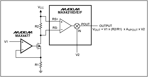
Figure 1. A generic 1V analog multiplier using the MAX4210D/E/F and MAX4477.
For the purposes of this application note, we will use the MAX4210E as our example; note, however, that the MAX4210D and MAX4210F can also be used to build a generic analog multiplier.
In the Figure 1 circuit, the voltage input V1 is converted into a current by the op amp, the MOSFET, and the resistor R1; resistor R2 then converts it into a smaller voltage. This smaller voltage is applied to the differential input of the MAX4210E. The maximum input sense voltage that can be applied to the MAX4210E is 150mV. R1 and R2 values should be chosen accordingly; specifically, R1 = 1kΩ and R2 = 150Ω. The power supply VCC of the entire circuit is 5V. The MAX4210E has a gain of 25V/V. Therefore, the full-scale output value is 3.75V.
The op amp should be chosen such that its input common-mode voltage range includes ground and its precision is superior to the MAX4210E. At 25°C, the MAX4210E has a total output error that is within ±1.5% of its full-scale output (FSO) range. The MAX4477 features an ultra-low bias current in the pA region, an input voltage offset within 350µV, and CMRR of at least 90dB; therefore, its error contribution is negligible versus the contribution of the MAX4210E.
Figure 2 shows a graph of the results of the first set of measurements, where the input V2 is kept constant to 0.9V and the input V1 swings from 0 to 1V in 100mV increments.

Figure 2. VOUT versus V1 with V2 = 0.9V.
The calculated gain error is 0.8%, and the total output error is 0.6% of the FSO. Gain error is calculated as the difference, expressed in percentage, between the measured and ideal curves' slopes with respect to the ideal curve's slope. Each slope is determined by the two-point measurement with linear assumption. Total output error is the maximum difference between the measured and ideal curves with respect to the FSO value of 3.75V, expressed as percentage.
Figure 3 shows a graph of the second set of measurements, where the input V1 is kept constant to 0.9V and the input V2 swings from 0 to 1V in 100mV increments. The calculated gain error is 0.81%, and the total output error is 0.58% of FSO.
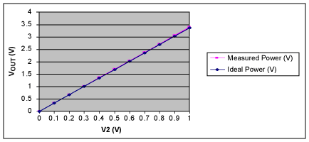
Figure 3. VOUT versus V2 with V1 = 0.9V.
Both gain error and total output error are within the specification of the MAX4210 for both sets of measurements.
Conclusion
To achieve accurate power management, some applications require load-power monitoring instead of just load-current monitoring. Capable of monitoring both load current and source voltage, the MAX4210D/E/F are ideal for battery-powered applications in which the supply voltage can be provided by either a battery pack or AC adapter. The circuit presented in this application note uses the MAX4210D/E/F to build a generic analog multiplier that is capable of multiplying two 0 to 1V signals to ensure accurate power management.