Trimless IF VCO: Part 2: New ICs Simplify Implementation
Abstract
Presents a family of IF voltage-controlled oscillators (VCOs) to cover the frequency range from 45MHz to 650MHz. The ICs are in 6-pin SOT23 packages. Phase noise is -100dBc/Hz for the MAX2608 at 300MHz to 500MHz. An off-chip inductor sets the operating frequency. The output stage can be matched with resistors or lossless techniques.
Additional Information: Trimless IF VCO: Part 1: Design Considerations
A new family of integrated circuits can ease the task of developing compact, fixed-frequency voltage-controlled oscillators (VCOs) for IF applications.
Designing a VCO for use with a fixed intermediate frequency (IF) can be daunting. Fortunately, VCO ICs from Analog Devices (MAX2605-MAX2609) can simplify the task. Compared to conventional discrete-device VCOs, the Analog Devices parts cost less and require less PC board space.
In a traditional IF VCO design, the oscillator core and the output buffer stage are formed by discrete transistors, resistors, capacitors, and inductors (Figure 1). The tank is built from a network consisting of the frequency-setting inductor, varactors, coupling capacitors, and feedback capacitors. The output stage uses reactive elements to match the output impedance to a particular load impedance.
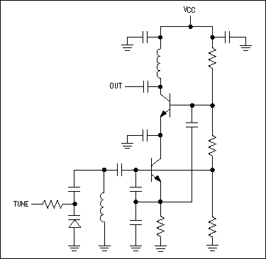
Figure 1. This schematic shows an IF VCO implemented with discrete circuit elements.
To ensure a successful design, the component values not only must establish a desired nominal oscillation frequency, but they must also guarantee an adequate tuning range, proper biasing, oscillator startup under all conditions, and proper output-stage performance. Problems can occur even with a good first-order design because of the trade-off that exists among current consumption, startup margin, frequency tuning range, and phase noise.
A major disadvantage of discrete IF VCO designs is the amount of PC board area required. Much effort must be expended in optimizing the layout to below 6mm x 10mm. Furthermore, the PC board layout has a critical effect on the VCO's performance and design accuracy. The layout contains parasitic capacitances and inductances that affect the oscillation frequency and must therefore be taken into account to implement the oscillator properly. Parasitic elements often bring about an undesired shift in the nominal oscillation frequency, which causes greater design-centering errors and ultimately forces a need for greater tuning range to account for those errors.
The MAX2605-MAX2609 IF VCO family offers a better alternative. These five ICs are designed for low-power, fixed- and single-frequency, portable wireless applications with IF frequencies in the 45MHz to 650MHz range. Much of the required circuitry is included on-chip; only the tank inductor (which establishes the oscillation frequency) is external.
Once you choose the correct external inductance value, the IC guarantees that some level within the tuning-voltage range (+0.4VDC to +2.4VDC) will tune in the corresponding frequency. The IC's tuning-voltage input can be driven directly from the loop-filter output following a phase-locked loop (PLL). MAX2605-MAX2609 ICs are designed for supply voltages in the +2.7VDC to +5.5VDC range, and the supply voltage connection does not require special regulation for proper operation. Each IC comes in a tiny, 6-pin, plastic SOT23 package (Figure 2).

Figure 2. The MAX2605-MAX2609 IF VCO ICs come in a 6-pin surface-mount SOT23 package designed to occupy minimum PC board space.
The MAX2605 tunes from 45MHz to 70MHz, with -117dBc/Hz phase noise at 100kHz from the carrier. For the other devices, these parameters are 70MHz to 150MHz tuning with -112dBc/Hz phase noise at 100kHz from the carrier (MAX2606), 150MHz to 300MHz with -107dBc/Hz (MAX2607), 300MHz to 500MHz with -100dBc/Hz (MAX2608), and 500MHz to 650MHz with -93dBc/Hz (MAX2609).
The frequency tuning range, biasing, startup, and other oscillator characteristics are all managed within the IC, eliminating the design headaches typically associated with VCO design. An on-chip varactor and capacitors simplify IF VCO design by eliminating the need for external tuning elements. A graph of inductance versus oscillation frequency (see the MAX2605-MAX2609 data sheet) further simplifies the task of choosing an external inductor.
The MAX2605 family provides several important new benefits for RF designers. The ICs are designed to create VCOs that are trimless and do not need external adjustments. To accommodate the anticipated range of system IFs found in dual-conversion systems, they are designed to cover a wide range of application frequencies. In addition, they have a flexible output interface to help reduce the cost of IF VCOs and shrink the size of the final design.
Because the MAX2605-MAX2609 represent a new concept in VCOs, they required a fundamentally new circuit approach to achieve the product objectives. Analog Devices devised an oscillator scheme based on the reliable and flexible Colpitts oscillator structure. This topology was adapted so that all the oscillator circuit elements (except the inductor) could be integrated within the IC. Integrating nearly the entire oscillator on-chip provides all the desired operating objectives of a good VCO: proper oscillator startup, wide frequency range, required tuning characteristics for trimless operation, controlled current consumption, and biasing that was independent of temperature and the power-supply voltages.
An off-chip inductor allows the VCO to be applied over a very wide range of operating frequencies. On-chip capacitance remains the same, but changing external inductance values modifies the resonant frequency of the oscillator tank circuit. If the inductor has a minimum quality factor (Q), the phase-noise and startup behavior can be guaranteed (Figure 3).

Figure 3. This simplified circuit diagram of the MAX2605-MAX2609 VCO ICs shows that only an external inductor is necessary to complete the resonant circuit that sets the oscillation frequency.
To implement this new approach, the IC technology needed a full complement of active and passive elements to support construction of the oscillator circuit shown. Specifically, the process technology had to provide high-frequency transistors, high-Q capacitors, high-Q varactor diodes with high capacitance ratios, and PNP or PMOS devices.
The MAX2605-MAX2609 are fabricated by means of a silicon BiCMOS process developed specifically for RF ICs that include monolithic oscillator structures. This process features PNP, NMOS, and PMOS devices, NPN transistors with transition frequencies (fT) of 25GHz, low-series-resistance varactor diodes with better than a 2:1 capacitance ratio (for tuning voltages from 0.4V to 2.4V), very-high-Q metal-insulator-metal (MIM) RF capacitors, precision-thin film resistors, and three layers of metal.
This full complement of devices allowed implementation of the complete IC. The VCO design required careful and extensive computer simulations, including multiple design iterations between various aspects of performance to ensure that all specifications and requirements could be guaranteed over all operating conditions.
Finally, to guarantee that the oscillator possessed a sufficient frequency-tuning range to account for the shift in operating frequency caused by component tolerances, Analog Devices elected to perform production testing on the devices and to guarantee a set of frequency limits. These limits provide MAX2605-MAX2609 users with a guaranteed set of high- and low-frequency tuning limits (fMAX and fMIN), in which passing ICs have a frequency of oscillation (fOSC) < fMIN at a tuning voltage (VTUNE) of 0.4V, and fOSC < fMAX at VTUNE = 2.4V. Assuming an external inductor with ±2% tolerance, including temperature drift, and a small design centering error (<0.5%), this testing guarantees that the VCO always tunes to the operating frequency selected by the inductor, without adjustment of the external inductance value. The result is a trimless VCO design.
MAX2605-MAX2609 applications are highly simplified and easy to understand. Two simple steps are involved:
- Select and implement an external inductance to set the desired oscillation frequency.
- Match the output stage resistively or reactively to the load (Figure 4).

Figure 4. This simple schematic represents a typical application for the MAX2605-MAX2609 VCO IC.
The nominal operating frequency (fNOM) desired for the VCO is determined solely by the effective external inductance value at IND (pin 1), as determined by a curve (Figure 5).

Figure 5. This plot contains values of the required total tuning inductance (LF) as a function of desired oscillation frequency (150MHz to 300MHz) for the MAX2607 VCO IC.
The inductance value (LF) required for a desired operating frequency will not necessarily coincide with any of the standard values for surface mount technology (SMT) inductors, which typically increase in steps that differ by a factor of approximately 1.2. To achieve the desired value in such cases, the inductance must be constructed from two inductors: LF1 and LF2. LF1 should be chosen as the nearest standard value below the desired value. Then, choose LF2 as the nearest standard value just less than LF - LF1. LF1 should adhere to the minimum Q requirements, but LF2 can be implemented as a lower-cost thin-film SMT type. Because its value is less than 20% of the total, its lower Q has only a small effect on the overall Q.
It is also permissible to adjust the total inductance value by implementing small amounts of inductance with PC board traces. For MAX2608/MAX2609 circuits, the inductance value for LF2 is sometimes implemented more precisely as a PC board trace shorted to ground than as an SMT inductor. Once the required inductance value is established at pin IND, the VCO is guaranteed to tune to this oscillation frequency over all component variations, operating temperatures, and supply voltages.
MAX2605-MAX2609 VCOs include a differential output amplifier after the oscillator core. The amplifier stage provides valuable isolation and offers a flexible interface to IF functions such as a mixer and/or a PLL prescaler. The output can be taken single-endedly or differentially, but the maximum output power and the lowest harmonic output are achieved in the differential-output mode. Both open-collector outputs (OUT- and OUT+) require a pullup element to the collector voltage (VCC). The output stage can be applied with a pullup resistor or inductor. A pullup resistor is the most straightforward method of forming an interface to the output and works well in applications that operate at lower frequencies or need only a modest voltage swing.
A reactive power match is required for operating frequencies above the 3dB bandwidth of the load-resistance/capacitance network and/or when a greater voltage swing or output power is desired. The matching network is a simple circuit with a shunt inductor and a series capacitor. To provide DC bias for the output stage, the inductors are connected from OUT- and OUT+ to VCC, and the series capacitors are connected from OUT- and OUT+ to the load. Values for the inductor and the capacitor are chosen according to the operating frequency and load impedance. The output is applied as any conventional differential output. The only constraints are the need for a pullup to VCC and a limit to the voltage swing at OUT- and OUT+.
A comparison of the design time required to apply each approach reveals a dramatic difference. The classical/ discrete approach shown is very design-intensive, and the successful development of a discrete IF VCO can take many weeks. Several iterations are likely before reaching a robust, manufacturable design. On the other hand, the MAX2605-MAX2609 let you design the VCO in minutes and then verify and test it in an afternoon!
Because the MAX2605-MAX2609 solve the problems of frequency tuning range, biasing, and startup, they completely eliminate the difficult tasks typically associated with a VCO design. You only need to select an external inductance value based on the desired oscillation frequency, and the output load. This task is accomplished easily by reading the desired inductance value from a graph supplied on the MAX2605-MAX2609 data sheet.
In bill-of-materials cost, the MAX2605-MAX2609 are comparable to the traditional discrete IF VCOs. As for manufacturing, Analog Devices' parts can support even less expensive IF VCOs, as a consequence of having fewer components to place and a $0.03 savings per component.
A similar article appeared in the August 2000 issue of Microwaves & RF magazine.