Transmit Pulse Control on the DS26518 T1/E1/J1 Transceiver
Abstract
As network-protection components are added to a system and/or signals must be routed through connectors and other PC-board requirements, sometimes it is necessary to manipulate the transmit waveform. This application note explains how the DS26518 T1/E1/J1 transceiver contains precise methods for making minor or major changes to the output pulse. The note also describes how to access factory test registers that allow a designer to modify the transmit waveform to meet a wide variety of application requirements.
T1 and E1 Transmit Waveform: Programmable Sections
The DS26518 registers provide control for the transmit pulse in two major areas: amplitude and timing. T1 and E1 transmit pulses are divided into sections, each of which can be manipulated to provide the desired waveform. Figure 1 shows how the T1 pulse is divided and the registers that control each section. Figure 2 provides the same information for the E1 pulse.
T1 and E1 Transmit Waveform: Amplitude Control
The amplitude of the DS26518 transmit pulse can be controlled in two ways:
- Adjusting the DAC Gain
- Partial Waveform Level Adjustment
The L1TXLAE register bits DAC[3:0] provide positive and negative adjustment of all the T1 or E1 levels simultaneously.
The WLA[3:0] bits of the Level Adjustment registers provide fine-tuning of specific sections of the waveform. The step size of the voltage level will change in proportion to the programmed DAC gain. If the DAC gain is increased by 10%, then the step sizes will also increase by 10%.
T1 and E1 Transmit Waveform: Timing Control
The timing of the DS26518 transmit pulse levels is controlled by the CEA[2:0] bits of the Level Adjustment registers. Each edge can be moved in both positive and negative directions in increments of 1/32 of TCLK.
General Recommendations
Modifying the DAC gain is the easiest way to control the amplitude of the transmit pulse, because the DAC gain will control the entire waveform with only one register change. Using the DAC gain first will allow for minimal, if any, modifications of the individual Level Adjustment registers. The maximum output of the DAC will be affected by VDD. At lower levels of VDD, the maximum DAC gain setting may be unattainable. Changing VDD will also affect the maximum voltage attainable by the line driver's output stage.
Negative values do not use signed integer representation. The MSB is the sign bit and the LSBs represent magnitude irrespective of sign. For example, a -3 in a WLA[3:0] register would be 1011b (bit 3 set to 1 means negative, 011 in the next 3 bits is magnitude 3), not 1101b (4-bit signed integer representation).
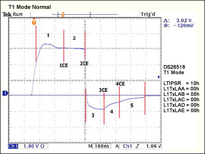
Figure 1. T1 pulse control sections.
T1 Pulse-Control Sections
| Overshoot (1) | Register L1TXLAA WLA[4:0] |
| Clock Edge (1CE) | Register L1TXLAA CEA[2:0] |
| (1CE) = Clock Edge transition from Overshoot to Plateau | |
| Plateau (2) | Register L1TXLAB WLA[4:0] |
| Clock Edge (2CE) | Register L1TXLAB CEA[2:0] |
| (2CE) = Clock Edge transition from Plateau to Falling Edge | |
| Undershoot (3) | Register L1TXLAC WLA[4:0] |
| Clock Edge (3CE) | Register L1TXLAC CEA[2:0] |
| (3CE) = Clock Edge transition from Falling Edge to end of Undershoot (3) | |
| Undershoot (4) | Register L1TXLAD WLA[4:0] |
| Clock Edge (4CE) | Register L1TXLAD CEA[2:0] |
| (4CE) = Clock Edge transition from end of Undershoot (3) to end of Undershoot (4) | |
| Undershoot (5) | Register L1TXLAC WLA[4:0] |

Figure 2. E1 pulse control sections.
E1 Pulse-Control Sections
| Overshoot (1) | Register L1TXLAA WLA[4:0] |
| Clock Edge (1CE) | Register L1TXLAA CEA[2:0] |
| (1CE) = Clock Edge transition from Overshoot to Plateau | |
| Plateau (2) | Register L1TXLAB WLA[4:0] |
| Clock Edge (2CE) | Register L1TXLAB CEA[2:0] |
| (2CE) = Clock Edge transition from Plateau to Falling Edge | |
| NOTE: Registers L1TXAC, L1TXAD, and L1TXAE are not used in E1 mode. | |
LIU Test-Register Descriptions
Table 1 provides the register address and description for LIU 1. These registers are duplicated for LIUs 2 through 8.
Table 2 provides the addresses for all of the LIU test registers.
| Address | Abbr. | Description |
| 1011h | L1TXLAA | LIU 1 Tx Level Adjust A (Test Register) |
| 1012h | L1TXLAB | LIU 1 Tx Level Adjust B (Test Register) |
| 1013h | L1TXLAC | LIU 1 Tx Level Adjust C (Test Register) |
| 1014h | L1TXLAD | LIU 1 Tx Level Adjust D (Test Register) |
| 1015h | L1TXLAE | LIU 1 Tx Level Adjust E (Test Register) |
| LIU | Address Range |
| 1 | 1011–1015h |
| 2 | 1031–1035h |
| 3 | 1051–1055h |
| 4 | 1071–1075h |
| 5 | 1091–1095h |
| 6 | 10B1–10B5h |
| 7 | 10D1–10D5h |
| 8 | 10F1–10F5h |
Detailed LIU Test-Register Documentation
The register address and description for LIU 1 are provided below. These registers are duplicated for LIUs 2 through 8.
| Register Name | L1TXLAA |
| Register Description | LIU Tx Level Adjust A (Overshoot Voltage) |
| Register Address | 1011H |
| Read/Write Function | R/W |
| Bit # | 7 | 6 | 5 | 4 | 3 | 2 | 1 | 0 |
| Name | WLA4 | WLA3 | WLA2 | WLA1 | WLA0 | CEA2 | CEA1 | CEA0 |
| Default | 0 | 0 | 0 | 0 | 0 | 0 | 0 | 0 |
Bits 7 to 3: Transmit Waveform Levels Adjust for Output Level 1 (WLA[4:0])
Moves magnitude from default ±360mV.
Bit 7 = sign bit ("1" means negative)
Bits 6 to 3 = magnitude (unsigned), i.e., 20mV is LSB step size
Bits 2 to 0: Clock Edge Adjust (CEA[2:0])
Moves clock edge ±3 32x-clks from default.
<2> = sign bit ("1" means negative)
<1:0> = number of 32x-clks to move (unsigned)
| Register Name | L1TXLAB |
| Register Description | LIU Tx Level Adjust B (Plateau Voltage) |
| Register Address | 1012H |
| Read/Write Function | R/W |
| Bit # | 7 | 6 | 5 | 4 | 3 | 2 | 1 | 0 |
| Name | WLA4 | WLA3 | WLA2 | WLA1 | WLA0 | CEA2 | CEA1 | CEA0 |
| Default | 0 | 0 | 0 | 0 | 0 | 0 | 0 | 0 |
Bits 7 to 3: Transmit Waveform Levels Adjust for Output Level 2 (WLA[4:0])
Moves magnitude from default ±360mV.
Bit 7 = sign bit ("1" means negative)
Bits 6 to 3 = magnitude (unsigned), i.e., 20mV is LSB step size
Bits 2 to 0: Clock Edge Adjust (CEA[2:0])
Moves clock edge ±3 32x-clks from default.
<2> = sign bit ("1" means negative)
<1:0> = number of 32x-clks to move (unsigned)
| Register Name | L1TXLAC |
| Register Description | LIU Tx Level Adjust C (Undershoot Voltage) |
| Register Address | 1013H |
| Read/Write Function | R/W |
| Bit # | 7 | 6 | 5 | 4 | 3 | 2 | 1 | 0 |
| Name | WLA4 | WLA3 | WLA2 | WLA1 | WLA0 | CEA2 | CEA1 | CEA0 |
| Default | 0 | 0 | 0 | 0 | 0 | 0 | 0 | 0 |
Bits 7 to 3: Transmit Waveform Levels Adjust for Output Level 3 (WLA[4:0])
Moves magnitude from default ±360mV.
Bit 7 = sign bit ("1" means negative)
Bits 6 to 3 = magnitude (unsigned), i.e., 20mV is LSB step size
Bits 2 to 0: Clock Edge Adjust (CEA[2:0])
Moves clock edge ±3 32x-clks from default.
<2> = sign bit ("1" means negative)
<1:0> = number of 32x-clks to move (unsigned)
| Register Name | L1TXLAD |
| Register Description | LIU Tx Level Adjust D (Undershoot Voltage #2) |
| Register Address | 1013H |
| Read/Write Function | R/W |
| Bit # | 7 | 6 | 5 | 4 | 3 | 2 | 1 | 0 |
| Name | WLA4 | WLA3 | WLA2 | WLA1 | WLA0 | CEA2 | CEA1 | CEA0 |
| Default | 0 | 0 | 0 | 0 | 0 | 0 | 0 | 0 |
Bits 7 to 3: Transmit Waveform Levels Adjust for Output Level 4 (WLA[4:0])
Moves magnitude from default ±360mV.
Bit 7 = sign bit ("1" means negative)
Bits 6 to 3 = magnitude (unsigned), i.e., 20mV is LSB step size
Bits 2 to 0: Clock Edge Adjust (CEA[2:0])
Moves clock edge ±3 32x-clks from default.
<2> = sign bit ("1" means negative)
<1:0> = number of 32x-clks to move (unsigned)
| Register Name | L1TXLAE |
| Register Description | LIU Tx Level Adjust E (Undershoot Voltage #3) |
| Register Address | 1015H |
| Read/Write Function | R/W |
| Bit # | 7 | 6 | 5 | 4 | 3 | 2 | 1 | 0 |
| Name | WLA4 | WLA3 | WLA2 | WLA1 | WLA0 | CEA2 | CEA1 | CEA0 |
| Default | 0 | 0 | 0 | 0 | 0 | 0 | 0 | 0 |
Bits 7 to 4: Transmit Waveform Levels Adjust for Output Level 5 (WLA[3:0])
Moves magnitude from default ±180mV.
Bit 7 = sign bit ("1" means negative)
Bits 6 to 4 = magnitude (unsigned), i.e., 20mV is LSB step size
Bits 3 to 0: DAC Gain Adjust (DAC[3:0])
The following settings change the gain of the DAC.
| DAC[3:0] | DAC Gain Value |
| 0000 | Nominal (default) |
| 0001 | +2.67% |
| 0010 | +5.34% |
| 0011 | +8.67% |
| 0100 | +11.34% |
| 0101 | +14.0% |
| 0110 | +17.34% |
| 0111 | +20.97% |
| 1000 | -2.1% |
| 1001 | -4.0% |
| 1010 | -6.0% |
| 1011 | -8.0% |
| 1100 | -10.0% |
| 1101 | -12.0% |
| 1110 | -14.0% |
| 1111 | -15.34% |
T1 and E1 Transmit Waveform Data
The following data is representative of the expected results for the DS26518. The data is a guideline for determining the range and method of using the Level Adjustment registers to control the amplitude and timing of the T1 and E1 transmit pulses. The data was taken at room temperature with 3.3V VDD.
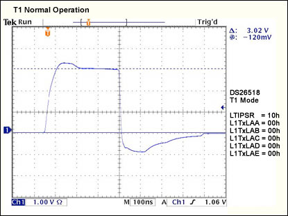
Figure 3.

Figure 4.

Figure 5.

Figure 6.

Figure 7.

Figure 8.
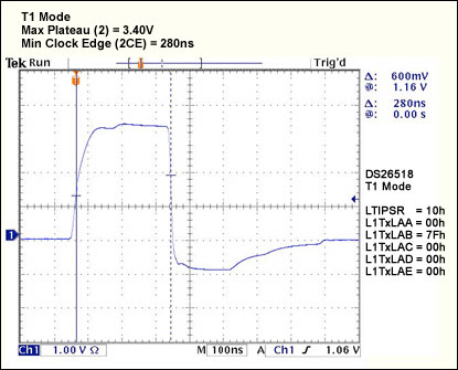
Figure 9.

Figure 10

Figure 11

Figure 12

Figure 13

Figure 14.

Figure 15.

Figure 16.
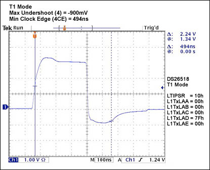
Figure 17.

Figure 18.

Figure 19.

Figure 20.

Figure 21.
Figure 22.

Figure 23.

Figure 24.

Figure 25.

Figure 26.

Figure 27.

Figure 28.

Figure 29.

Figure 30.

Figure 31.

Figure 32.

Figure 33.

Figure 34.

Figure 35.

Figure 36.

Figure 37.

Figure 38.

Figure 39.

Figure 40.

Figure 41.

Figure 42.

Figure 43.
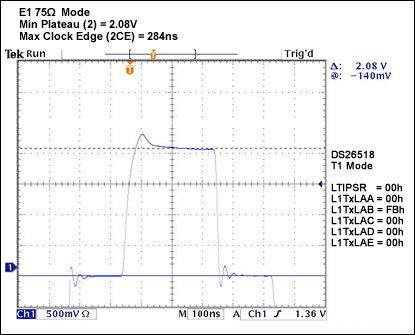
Figure 44.

Figure 45.
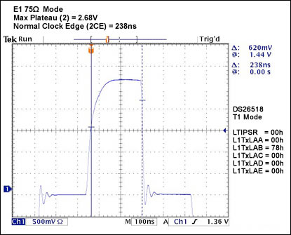
Figure 46.

Figure 47.

Figure 48.

Figure 49.

Figure 50.

Figure 51.