Solutions for Integrated Clock Sources Using the MAX9489/MAX9471 Multiple-Output Clock Generators
Solutions for Integrated Clock Sources Using the MAX9489/MAX9471 Multiple-Output Clock Generators
Abstract
Using an integrated multiple-output clock generator has many advantages over typical 'local' clock solutions. This article discusses the advantages of a centralized clock generator like the MAX9489 and the MAX9471 for system cost reduction, good signal integrity and elimination of interference. It includes board designs which illustrate how to overcome some basic design challenges with a central clock source.
The MAX9489/MAX9471 are multiple-output clock generators. The MAX9489 is designed for applications in SOHO routers and networking equipment and the MAX9471 is for consumer electronics.
Compared to typical 'local' clock solutions, a centralized clock generator has many advantages for applications with multiple ports and modules.
There are practical considerations when designing with a multiple-output clock generator. Guidelines presented here will demonstrate how a well-designed centralized clock source minimizes signal degradation, prevents noise interference, and reduces system cost. Block diagrams illustrate these applications.
Application Advantages of a Centralized Clock Generator
Today's network router/switch system must support more and more interface ports and modules. Each port or module usually requires a reference clock, typically generated by a local crystal or crystal oscillator associated with that port or module. As the number of ports and modules increases, the cost of the reference clock generation climbs. Such a local clock solution also makes it hard for the system to reconfigure the reference clocks for testing, interface power management, and up- or down-grading ports or modules. This design challenge applies to set-top box and digital TV applications.
Using a centralized clock generator is not new; it has been used in every PC motherboard. In the set-top box design, for example, more than 11 different interfaces and modules need different clocks. Instead of providing the reference clocks locally, the MAX9489 can generate all the required clocks for the routers and set-top boxes. By using an integrated multiple-output clock generator like the MAX9489 and MAX9471, you reduce system cost and increase the design's ability to control the system.
There are 15 LVCMOS-programmable clock outputs in MAX9489 and each clock output can select among 10 different frequencies for Ethernet, PCI, memory, and MCU. In the MAX9489, each clock output can be independently controlled through I2C. Also, the MAX9489's clock output frequencies can be moved up and down by 5% or 10%, which makes it easy for the system to do over-driving or under-driving tests. Figures 1 and 2 illustrate the system block diagrams of the MAX9489 in routers and the MAX9471 in set-up boxes, respectively.
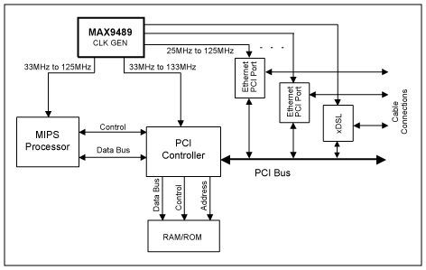
Figure 1. System block diagram of a SOHO router.

Figure 2. System block diagram of a set-top box.
Board Design Guidelines
Delivering the clocks across the circuit board without degrading the signal integrity is a challenge when using an integrated clock generator. Usually, the clock trace's length will be in the 3-inch to 9-inch range. For such a trace length, following the practice in motherboard design, the LVCMOS signaling can operate at a frequency as high as 150MHz. However, special care must be taken in board design. The two practical issues are: minimizing the rise/fall time degradation due to the long PCB trace, and preventing noise interference coupled from the other sources on the same board.
Minimizing Signal Degradation
To reduce the rise/fall time degradation, a 50Ω trace is often used and a 25Ω to 33Ω resistor, Rs, is inserted between the CLK output pin and the trace. Knowing the impedance of the driver's pull-up and pull-down transistors to be about 20Ω, inserting Rs makes the total output impedance of the LVCMOS driver match the 50Ω trace. The schematic of the driving circuit is shown in Figure 3.

Figure 3. LVCMOS output driving circuit.
The lengths of K and L are given in the following Table 1.
| K | L | |
| Trace Length at 33MHz | 0.1 to 1.0 inches | 2 to 13 inches |
| Trace Length at 100MHz | 0.1 to 1.0 inches | 2 to 9 inches |
The resistor, Rs, should be connected to the LVCMOS output pin by a K-inch trace. The optimal values of K and Rs can be determined by experiment or simulation. These values are the functions of the driver output impedance, trace impedance and length, parasitic components, and the termination impedance. If the output pin to termination is less than 2 inches, there is no need for Rs. When the clock frequency is higher than 100MHz, the clock trace length should be reduced further. To show the better signal integrity of the matched trace, we take a 100MHz clock from one of MAX9489's outputs and put it through a 5-inch 50Ω trace. Figure 4 shows the signal waveforms collected at different locations of the trace.

Figure 4. The waveform at LVCMOS output pin without trace.

Figure 5. The waveform at the termination of a 5-inch trace with Rs = 0Ω.

Figure 6. The waveform at the termination of a 5-inch trace with Rs = 33Ω and K = 0.5 inches.
As seen in Figures 4 through 6, the signal integrity improves considerably by adding Rs at a proper location.
Preventing Noise Interference
To resolve the second practical issue of preventing noise interference, we can reduce the mutual interference between clocks and other signals. The clock trace can be sandwiched by ground traces, as shown in Figure 7.

Figure 7. Clock trace layout with ground trace isolation.
EV Kits and I2C Programming
The MAX9489 EV (evaluation) kit is available upon request. If you do not have an I2C bus available, you can ask Maxim to provide an I2C programming interface board with the board ID (the part number) MAXSMBus.
References
- MAX9489 data sheet.
- MAX9471 data sheet.
- Intel technical specification, "CK00 Clock Synthesizer/Driver Design Guidelines."
- Eric Bogatin, Signal Integrity - Simplified, (Prentice Hall, New York, 2004).
- MAXSMBus data sheet.