Silicon-Bipolar IC Facilitates VCO Design
Abstract
The frequency of a voltage-controlled oscillator (VCO) varies with the voltage applied to its tuning port. Operating in a phase-locked loop (PLL), the VCO provides a stable local oscillator (LO) for frequency conversion in superheterodyne receivers. VCOs are also used in transmit chains, where they upconvert the baseband signal to a radio frequency (RF) suitable for transmission over the airwaves.
The frequency of a voltage-controlled oscillator (VCO) varies with the voltage applied to its tuning port. Operating in a phase-locked loop (PLL), the VCO provides a stable local oscillator (LO) for frequency conversion in superheterodyne receivers. VCOs are also used in transmit chains, where they upconvert the baseband signal to a radio frequency (RF) suitable for transmission over the airwaves (Figure 1).
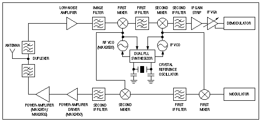
Figure 1. VCOs appear as part of the PLLs in this typical superheterodyne receiver.
Design Considerations
The VCO designer must consider several important performance parameters:
- Output level in dBm (dB relative to 1mW)
- Output harmonic level in dBc (dB relative to carrier power)
- Tuning sensitivity in Hz/V
- Load pulling of oscillation frequency in Hz p-p (for a given load voltage standing-wave ratio (VSWR) rotated through 360°)
- Frequency pushing, in Hz/V, of bias-supply change
- VCO phase noise, in dBc/Hz, at a given offset frequency
The following paragraphs discuss each parameter in turn.
Output Level
In typical superheterodyne receivers, the VCO output must drive a mixer as well as a PLL synthesizer's RF prescaler. This requirement is commonly met with a buffer amplifier, which provides load isolation as well as greater drive capability.
Output Harmonic Level
Output harmonic level is a measure of the VCO energy at harmonics of the oscillation frequency. These harmonics, common at levels below -15dBc, are generated by the nonlinear self-limiting of active devices in the oscillator. Oscillators with large amounts of excess gain (greater than the amount necessary to offset all losses at resonance) will limit more severely, thereby generating a greater harmonic content in the output waveform. The designer must balance the need to keep harmonic levels low with the need for enough excess gain to ensure oscillator start-up.
Tuning Sensitivity
Tuning sensitivity is a system-level parameter that relates the maximum available tuning voltage to the required tuning-frequency range, in units of Hz/V. It is inversely proportional to the loaded Q, which is the loaded oscillator tank's quality factor. Higher tuning sensitivities require oscillators with lower loaded Qs.
The variation of tuning sensitivity over the tuning-frequency range is another important consideration. If a VCO's tuning sensitivity varies dramatically over the tuning band, the PLL synthesizer's performance suffers. The VCO is the highest gain device in a typical PLL, with tuning sensitivities in the tens of MHz/V. This amount of gain can cause unwanted modulation side-bands in response to noise at the tuning port; therefore, tuning-port noise must be minimized.
Load Pulling
Load pulling measures the sensitivity of a free-running VCO to load variations at the VCO output. Measurement requires a load-impedance mismatch and a variable-length transmission line. Connect the VCO to the mismatched load, and vary the phase angle (between VCO and load) through 360° by changing the length of the transmission line. Measure the resulting peak-to-peak frequency change. VCO load pulling is specified as the maximum peak-to-peak frequency shift at a given load VSWR, rotated through 360°. Equation 1 shows the relationship between load VSWR and load-impedance mismatch:
Equation 1:
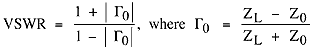
where:
VSWR = voltage standing-wave ratio
Γ0 = load-reflection coefficient: the ratio (at the load) of the incident voltage wave to the reflected wave
ZL = load impedance
Z0 = the transmission line's characteristic impedance
Using buffer amplifiers is the most common technique for reducing a free-running VCO's sensitivity to load variations.
Frequency Pushing
Frequency pushing measures a free-running VCO's sensitivity to variations in its bias-supply voltage. To measure the VCO's sensitivity, vary the supply voltage over a given range while measuring the VCO frequency. Divide this frequency shift by the voltage change to determine sensitivity in Hz/V. Well-designed VCOs have pushing factors between 5% and 10% of the main tuning-line sensitivity. An example of a device with excellent pushing performance is Maxim's MAX2620 VCO, which has a tuning-port sensitivity of 10.4MHz/V and a pushing sensitivity of only 71kHz/V. Pushing sensitivity for the MAX2620 is less than 1% of the tuning-port sensitivity.
VCO Phase Noise
Phase noise in a free-running VCO relates the noise-sideband level to the carrier-power level. In a typical measurement, observe the VCO output on a spectrum analyzer while measuring the noise level in a 1Hz bandwidth at a given frequency offset from the carrier. Modern spectrum analyzers equipped with a particular firmware option can generate a graph showing single-sideband phase noise versus offset frequency by taking multiple measurements with various offsets, and making appropriate changes to the internal IF bandwidth in each case.
Oscillators with very low phase noise (crystal oscillators, for example) cannot be measured by a spectrum analyzer because the phase-noise limit for its LO is too high. The 8561 RF spectrum analyzer from Hewlett Packard, for instance, specifies phase-noise limits of -80dBc/Hz at 100Hz, -97dBc/Hz at 1kHz, -113dBc at 10kHz, -113dBc at 30kHz, and -113dBc at 100kHz. A typical crystal oscillator, on the other hand, has 30dB to 40dB less phase noise at each of these offset frequencies. For such high-quality oscillators, an accurate phase-noise measurement requires more sophisticated techniques.
Several key factors affect a free-running VCO's phase noise. All are included in Equation 2, a formula for estimating an oscillator's single-sideband noise.
Equation 2:
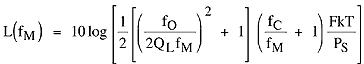
where:
L(fM) = single-sideband phase noise in dBc/Hz, as a
function of offset frequency from the carrier
fO = output frequency in Hz
QL = loaded resonator Q (resonator tank circuit
with active load and all parasitic elements)
fC = corner frequency in Hz for flicker noise in the
active oscillation device
fM = offset from the carrier in Hz
PS = the active oscillation device's oscillation-
signal power, in watts
F = the active device's in-circuit noise factor
(with the resonator tank and all parasitic
elements)
k = Boltzmann's constant: ~1.38 x 10⁻²³ J/°K
T = temperature in degrees Kelvin (°K)
In this formula, loaded-resonator Q is the dominant design parameter affecting phase noise. Low-noise design dictates that this parameter be maximized to meet tuneability requirements. A high loaded-resonator Q requires the use of resonant-tank components with high unloaded Q. Under these conditions, the tank's load should couple just enough energy to the rest of the circuit to start and sustain oscillations. The resonator's loaded Q can easily be less than a tenth of its unloaded Q.
The corner frequency for flicker noise is device dependent; low-noise design demands devices with a low flicker corner. The flicker-noise corner makes bipolar processes the best choice for low-noise oscillator design. GaAs devices cannot compete because their noise corner is from two to three orders of magnitude greater than that of Si-bipolar devices.
Because the value of the in-circuit noise factor depends on the device as well as its external circuit, low-noise design requires that both be optimized. Adjusting the oscillation-signal power allows some control over phase noise, but the premium on bias current in today's hand-held wireless phones usually prohibits large changes in the oscillator section's current drain.
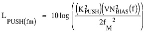
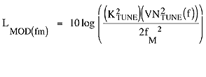
Equation 3 describes phase noise intrinsic to the oscillator. Adding to this are the modulation-noise sidebands produced by noise on the tuning line (see Equation 4).
Equation 3:
Equation 4:
where:
LPUSH(fm) = single-sideband phase noise (in dBc/Hz)
due to noise voltage modulating the VCO through the bias line
LMOD(fm) = single-sideband phase noise (in dBc/Hz)
due to noise voltage modulating the VCO through the tuning line
K2PUSH = supply-pushing sensitivity, in Hz/V
K2TUNE = oscillator tuning gain, in Hz/V
VN2BIAS(f) = noise-voltage density on the bias line as
a function of frequency (nV/Hz)
VN2TUNE(f) = noise-voltage density on the tuning line
as a function of frequency (nV/Hz)
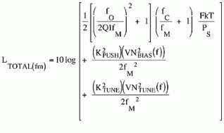
Adding equations 2, 3, and 4 results in equation 5, an estimate of the VCO's total single-sideband phase noise:
Equation 5:
Limitations in the previously mentioned VCO parameters can lead to degradation of system-level performance. For example, the power amplifier (PA) in a cellular phone is activated only when a voice signal is present. This switching causes the PA's input impedance to vary considerably, which in turn presents a problem for the RF VCO driving the transmit chain. Unless the VCO is isolated from the load variations (typically by a load buffer), its frequency variations can cause the PLL to slip cycles or even lose phase lock.
Another problem is the drastic change in supply current caused by the PA's off/on cycling. Typical PAs for GSM, DCS1800, and DCS1900 handsets can draw over 1A, and the current switching causes voltage changes on the VCO's bias line. The result of these bias-voltage changes and the pushing factor is unwanted modulation sidebands that fall outside of the PLL synthesizer's loop bandwidth. The VCO's bias voltage must be stabilized to eliminate this problem.
The unfaded bit-error rate (BER) in digitally modulated systems is limited by the net phase noise of all signal generators in the transmit and receive paths, with the RF VCO in the PLL synthesizer (usually) as the dominant contributor. The classic waterfall curve in Figure 2 shows the effect of phase noise. Beyond a certain level of Eb/NO (Eb is energy per bit; NO is additive white Gaussian noise density), the BER remains essentially constant. For a more robust communication link, lower the unfaded BER by reducing phase noise in the PLL synthesizer's RF VCO.
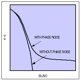
Figure 2. For higher values of energy per bit divided by additive white Gaussian noise density (Eb/NO), the bit-error rate (BER) is essentially constant.
Phase noise is a primary concern for digital-modulation techniques in which information is encoded by modulating the carrier phase. One such technique is quadrature phase-shift keying (QPSK). Analogous to in-phase/quadrature modulation in the analog domain, QPSK allows transmission of a given bit stream at half the data rate by encoding pairs of bits at each of four different phases. Each phase (π/4, 3π/4, 5π/4, and 7π/4 in Figure 3a) is represented as a point in signal space that is spread into a cloud by the presence of additive white Gaussian noise (AWGN) in the system.
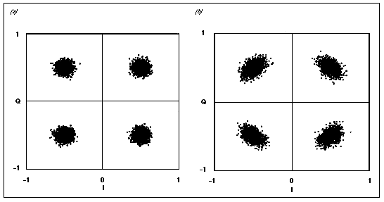
Figure 3. The signal constellation for a QPSK signal with Gaussian noise (a) is degraded by the addition of 5° of RMS phase variance (b), producing a distortion that can raise the BER.
Figure 3b shows the same QPSK constellation with the same AWGN, but with 5° of RMS phase variance added. Phase variance deforms the four constellation regions into arcs that reduce the distance between regions. This effect increases the probability of a symbol error at the demodulator, and an increase in symbol errors increases the BER. Thus, the amount of phase variance that can be tolerated depends on the demodulator design and on the performance required in the communication link. Equation 6 shows the relationship between integrated phase variance and phase noise:
Equation 6:
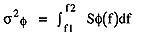
where:
f1, f2 = frequencies over which the integral is evaluated (usually determined by the demodulator design)
σ2Φ = integrated phase variance in radians squared
SΦ(f) = phase-power spectral density in radians squared/Hz (twice the single-sideband phase noise for small angles)
√σ2Φ = integrated RMS phase error, in radians
Perhaps the most stringent restraint on an LO's phase noise is imposed by receiver desensitization. This effect occurs in cellular phones and other environments in which the receiver must detect a weak signal in the presence of a strong interferer. In Figure 4, a strong nearby interferer mixes with the LO's phase noise to produce noise sidebands that reduce the signal-to-noise ratio at the IF, thus desensitizing the receiver's ability to detect weak signals.
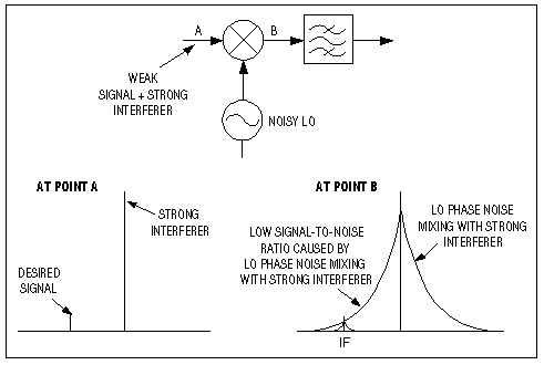
Figure 4. By mixing with the local-oscillator signal, a strong interfering signal generates noise sidebands that mask the signal of interest.
Earlier versions of the low-noise VCO were composed of discrete components: a specialized bipolar transistor with low corner frequency for flicker noise, a bias-voltage supply, and buffer amplifiers to provide load isolation and added output drive. The many passive chip components in the discrete circuit required a lot of PC board space, which is at a premium in today's small wireless handsets.
An Integrated Solution
Maxim's MAX2620 (Figure 5) integrates all the active functions of a discrete-component approach into a tiny, 8-pin µMAX® package. It includes a critical bipolar transistor with low corner frequency for flicker noise, fabricated in Maxim's exclusive Si-bipolar process featuring a 27GHz fT. The PC board area saved by higher-level integration simplifies PC board layout and shielding.
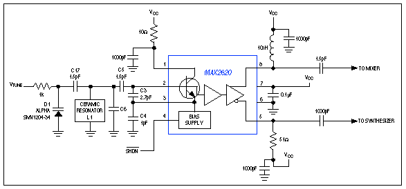
Figure 5. This typical operating circuit shows the use of a MAX2620 in building a VCO.
Besides the low-noise transistor, the MAX2620 includes a double buffer with two outputs (for load isolation), a bias generator, and convenient shutdown capability. This device operates from a +2.7V to +5.5V single supply and dissipates only 27mW at 3V. When operating at 900MHz, a load VSWR of 1.75:1 rotated over 360° produces a frequency shift of less than 163kHz. The MAX2620's internal bias-voltage generator greatly reduces the effect of bias-voltage variation on the oscillation frequency. At a 900MHz center frequency and a 3V to 4V supply-voltage change, the device achieves a 71kHz/V pushing sensitivity.
The MAX2620 has two outputs. One output, which generates -2dBm into a 50Ω load, typically drives a mixer's LO input. The other generates -12.5dBm into a 50Ω load and typically drives an integrated PLL synthesizer's RF prescaler input. Operating at 900MHz with a high-Q external tank circuit, the MAX2620 and its low-noise internal transistor produce low phase noise: -110dBc/Hz at 25kHz and -132dBc/Hz at 300kHz. The external tank allows designers to optimize tuneability and single-sideband phase noise for a given application.
To ensure oscillation start-up, the tank circuit's real-impedance magnitude should equal one-third to one-half of the oscillator device's negative real-impedance magnitude, and the tank's reactive component should be opposite in sign to that of the oscillator device. After start-up, gain compression lowers the oscillator's negative resistance until it achieves equilibrium with that of the resonant tank circuit.
Adding a varactor diode (voltage-tuned variable capacitor) to the tank circuit enables oscillator-frequency tuning, as long as the oscillator device exhibits an adequate negative resistance over the desired tuning range. The MAX2620 design is optimized in this respect.
The MAX2620 oscillator is also optimized for operation with low phase noise. Achieving the lowest phase noise possible requires the use of high-Q components such as ceramic transmission-line resonators (typical unloaded Q of 400) and high-Q inductors (typical unloaded Q of 180). To maximize the loaded Q in Figure 5, C5 and C17 should have the lowest value compatible with the desired frequency and tuning range. For 900MHz operation, C6 should be 1pF for the ceramic-resonator circuit and 1.5pF for the inductor circuit. Because a high-Q inductor's unloaded Q is lower than that of a ceramic resonator, the use of high-Q inductors (versus ceramic resonators) tends to degrade phase noise slightly. Phase noise for an inductor-based tank is -107dBc/Hz at 25kHz and -127dBc/Hz at 300kHz.
Both MAX2620 outputs have open collectors that require external components for pull-up to the supply voltage. Resistors of 50Ω match the outputs to a 50Ω system, but resistors rob output power. For maximum output power, use a pull-up inductor as shown at the buffer output in Figure 5. The inductor circuit's open-collector output impedance should be matched to the desired load impedance through an appropriate matching network.
A key factor in achieving optimum oscillator performance is the PC board layout. To minimize the effect of parasitic elements, remove the PC board ground plane under and around components that make up the resonant circuit. To minimize parasitic inductance, keep trace lengths as short as possible. Connect the decoupling capacitors (pins 1, 4, and 7 to ground) as close as possible to the MAX2620 package, with direct connections to the ground plane. The capacitors in Figure 5 must have an 0805 or smaller footprint.
As a cost-effective, low-power oscillator for the RF VCO in today's wireless headsets, the MAX2620 provides features that once required many discrete parts. Its double-buffered outputs provide load isolation, and its internal regulation cell provides isolation from power-supply fluctuations. Power dissipation with a +3V supply is just 27mW. The MAX2620 achieves very low phase noise, and its external tank lets the designer tailor an oscillator circuit to a given application.
References
1 Boyles, John W. "The Oscillator as a Reflection Amplifier: an Intuitive Approach to Oscillator Design," Microwave Journal, June 1986, pp 83-98.
2 Crawford, James A. Frequency Synthesizer Design Handbook, MA: Artech House, Inc., 1994.
3 Egan, W. Frequency Synthesis by Phase Lock. John Wiley & Sons, Inc., 1981.
4 Leeson, D. B. "A Simple Model of Feedback Oscillator Noise Spectrum," Proceedings of the IEEE, February 1966, pp 329-330.
5 MAX2620 Data Sheet, Rev. 0, July 1997, Maxim Integrated
6 Rhea, Randall W. Oscillator Design and Computer Simulation, Second Edition. Atlanta: Noble Publishing, 1995.
7 Temple, R. "Choosing a Phase Noise Measurement Technique-Concepts and Implementations," HP RF and Microwave Measurement Symposium, February, 1983.