PCB Layout Guidelines for the MAX14921 High-Accuracy 12-/16-Cell Measurement AFE
PCB Layout Guidelines for the MAX14921 High-Accuracy 12-/16-Cell Measurement AFE
Abstract
The MAX14921 analog front-end (AFE), combined with an analog-to-digital converter (ADC) and a voltage reference, form a high-performance, cost-effective solution for battery (cell stack) measurement. To achieve highest accuracy, care must be taken with the printed circuit board (PCB) layout. This application note provides a few layout suggestions that, when followed, help you to achieve the highest level of accuracy that your solution is capable of delivering.
Introduction
The MAX14921 is a high-performance building block, crucial in high-accuracy cell-stack measurement applications. This enhanced accuracy is especially important with new lithium phosphate cell chemistries, whose charge and discharge curves are exceptionally flat, particularly in the 65% to 95% state-of-charge (SOC) region. The superior accuracy derives from the MAX14921's unique sample-and-hold architecture, which minimizes both cell voltage acquisition errors and errors from sampling cells at different times.
Along with greater accuracy comes the need for greater care during design. This application note describes some simple, yet effective, layout guidelines to help you realize the benefits of this enhanced accuracy.
Mitigating Noise
The following noise-related guidelines are well known by those practiced in the art of modern PCB layout, so these are more reminders of those layout aspects most critical to noise management particular to the MAX14921.
Bypass Capacitors
It is well known that bypass capacitors are important circuit elements, good for filtering noise before it makes its way into an integrated circuit (IC). For greatest effectiveness, it is important to place the bypass capacitors as close to their IC power pins as is reasonable. Table 1 details the MAX14921's bypass capacitor requirements.
| Pin Name | Pin Number | Capacitor Value | Return |
| VL | 5 | 0.1µF | DGND (6) |
| VA | 12 | 1.0µF | AGND (11) |
| VP | 14 | 0.1µF | AGND (11) |
It can get crowded on the left side of the IC, where the digital SPI interface, the analog T1, T2, T3 inputs, the analog output, the power-supply pins, and some of the sampling capacitors vie for real estate. To ease congestion, recall that the space under the MAX14921 is available. Vias on the solder side of the PCB, under the MAX14921, can route signals as well as connect to capacitors placed there.
Keep the supply traces from the capacitors to their respective pins as short as is reasonable. For some layouts, this means putting capacitors on the solder side. If only one bypass capacitor can fit on the component side, it should be the pin 12 (VA) capacitor.
The subsequent figures illustrate some layout examples, taken from a 4-layer evaluation board. In these examples, top copper is red, layer 2 (green) is DGND, layer 3 (yellow) is V5V, and layer 4 (blue) is the bottom copper. This first example shows how VL is bypassed, presuming VL is at 3.3V. In Figure 1, copper continues past pin 5, under the MAX14921, where it vias to bypass capacitor C22 on the solder side of the board, under the MAX14921. The other side of the capacitor vias back up to layer 2, DGND.
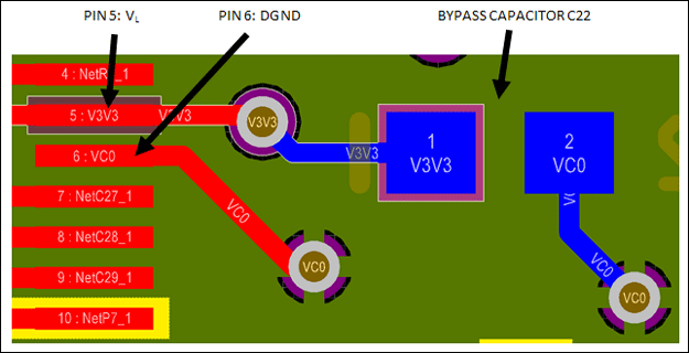
Figure 1. MAX14921 pin 5 bypass capacitor example.
Figure 2 shows how VP is bypassed. As in the case with pin 5, top copper continues past the IC pin under the MAX14921 and vias to a bypass capacitor under the IC. Since the return for pin 13 is AGND, the other side of C24 goes to pin 11 instead of attaching to the DGND plane.
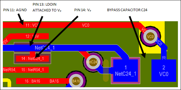
Figure 2. MAX14921 pin 14 bypass capacitor example.
Figure 3 shows how VA is bypassed. As explained below, it is advantageous to have the AGND signal (pin 11) parallel the AOUT signal (pin 10). For this reason, it is usually easiest to have the pin 12 bypass capacitor on the same side of the PCB as the MAX14921 itself. This maximizes the effectiveness of this bypass capacitor.
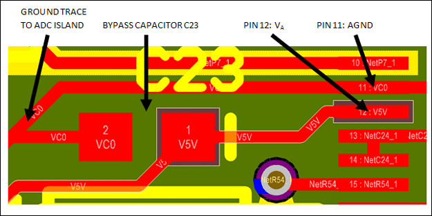
Figure 3. MAX14921 pin 12 bypass capacitor example.
ADC Island
Another technique to manage noise is to have separate ground islands under sensitive analog components. Figure 4 shows a separate ground island for the ADC, U3, and how pin 11 connects to it. The white outline highlight shows how the trace from the MAX14921 AGND pin attaches to the ADC ground island at the via just to the left of C20, a bypass capacitor dedicated to that ground island. The only connection between the DGND plane and the AGND net is the via at the top right of the ADC ground island, also highlighted in a white outline.
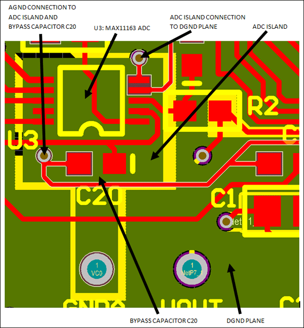
Figure 4. Ground island for the ADC (U3).
Connecting AOUT to the ADC
As part of the total solution, the MAX14921 AOUT signal (pin 10) connects to an ADC input. The layout in Figure 5 shows a good way to do this. The AOUT trace (highlighted) has ground relief (from layer 2, DGND) all the way to the RC filter composed of R2 and C25. In addition, the AGND trace from pin 11 parallels the AOUT trace. It is a good idea to leave footprints for an RC filter. A reasonable starting value for this filter is 220Ω with 220pF.
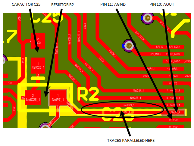
Figure 5. Connection from the AOUT pin to the ADC.
Filtering T1, T2, and T3
It is also a good idea to filter the T1, T2, and T3 analog inputs. If these signals come from temperature sensors, use an RC network such as 1kΩ and 10nF as a starting point. Otherwise, start with an RC network such as 220Ω and 2.2nF.
Digital Signal Separation
The MAX14921 has just a few digital signals, the SPI interface (SCLK, SDI, SDO, and #CS) along with the SAMPL pin and the EN pin (if these last two are used in the design). These digital signals need to be kept away from sensitive analog inputs and outputs, the most critical of which is the AOUT signal (pin 10). Ideally, keep these digital signals on a different layer than the analog, but this is not absolutely necessary if special care is taken to keep them separated.
Maintaining Accuracy
A bit of careful layout planning maintains cell-stack voltage accuracy on its way to the ADC.
Separating Power from Signals
The MAX14921 VP pin powers the front-end interface to the cell stack. It connects directly to the top of the battery stack, as does the CV16 pin (for a 16-cell stack). However, these connections need to be kept separate, starting as close to the battery as possible. Current flow in any wiring common to VP and CV16 will cause an IR drop that could reduce the accuracy of the voltage measured at CV16.
The same guideline holds true for VC0 and AGND. The current flow from AGND will cause an IR drop in any wiring common to both, degrading the accuracy of the signal at CV0. This is why the evaluation (EV) kit for the MAX14921 has separate connector pins for VP and CV16, as well as for CV0 and AGND.
Minimizing Stray Capacitance
The MAX14921 operates in two phases. The first phase acquires the cell voltages onto the sampling capacitors. The second phase transfers these voltages from the sampling capacitors to the ADC. During this second phase, any stray capacitance on the CT_ pins reduces voltage measurement accuracy through charge injection.
Practically, this means using short and thin traces as much as possible, between all the sampling capacitors and the MAX14921, as well as between the AOUT pin and the ADC input. Since the sampling capacitors are 0805 footprint, it may not be obvious how to keep all the traces as short as possible.
One effective technique is to place the sampling capacitors end-on and to give priority to keeping the connections to the CT_ pins as short as possible. The CB_ trace lengths will necessarily be longer. To compensate for this, an island in the ground plane under each capacitor attaches to its corresponding CB_ pin. This will minimize the stray capacitance from that sampling capacitor.
An example of this is shown in Figure 6, detailing the connections to the MAX14921 sampling capacitor pins on the bottom row (CT14, CB14, CT13, CB13, CT12, CB12, CT11, and CB11). Note, for example, how pin 29 (CT13) has a short trace to its sampling capacitor, but pin 30 (CB13), the highlighted trace, is longer. Also note how a separate ground island just below that capacitor also connects to the CB13 net through the via just below it.
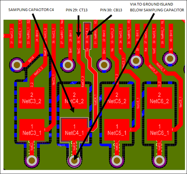
Figure 6. Minimizing stray capacitance at the sampling capacitors—Layer 3 (yellow) hidden to improve clarity.
Conclusion
This application note highlights a few simple guidelines during layout that can help ensure that you will obtain the submillivolt accuracies that a MAX14921 solution is capable of achieving. An example of the application of these guidelines is available for download.