Organic Land Grid Array (OLGA) and Its Applications
Abstract
This application note discusses Maxim Integrated’s OLGA and provides the PCB design and SMT assembly guidelines.
Introduction
The organic land grid array (OLGA) package is a leadless package with air cavity and organic substrate with patterned conductive traces. ASIC and LEDs with different wavelengths are integrated in the package depending on specific applications. All OLGAs are leadless packages where connections are made through the leads (terminal pin) on the bottom surface of the package. These leads can be directly soldered onto the PCB. Maxim Integrated ships OLGAs in tape-and-reel (T and R) format.
PCB Design
A well-designed and manufactured printed circuit board (PCB) is required for optimum manufacturing yields and product performance. Two types of land patterns are used for surface-mount devices (Figure 1): a) Solder mask-defined (SMD) pads have solder mask openings that are smaller than metal pads. b) Non-solder mask-defined (NSMD) pads have solder mask opening that are larger than the metal pads. Maxim recommends the use of NSMD pads since they provide larger metal areas for the solder to anchor to the edges of the metal pads. NSMD improves the solder joint reliability. Only one type of pad (NSMD or SMD) and one type of pad surface finish should be used on a given footprint.
- Land pattern: Each package code has one corresponding land pattern drawing. Please follow the corresponding package code.
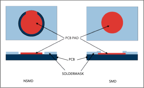
Figure 1. Illustration of NSMD and SMD land pad patterns.
Board Thickness
Units can be mounted on either the main PCB or flex PCB. Thin boards are recommended to prevent failure due to high stress on the package after SMT. In case of a need to go beyond below values, please contact a Maxim package engineer.
| Package Thickness (mm) | Main Board Thickness (mm) | Flex PCB (µm) |
| 1.0–1.4 | ≤ 0.6 | OK |
| > 1.4 | ≤ 0.85 | OK |
PCB Surface Finish
OSP (Organic Solderability Preservative), ENIG (Electroless Nickel/Immersion Gold), Electrolytic Nickel/Gold, ENEPIG (Electroless Nickel Electroless Palladium/Immersion Gold), Immersion Silver, and Immersion Tin finishes are used in the industry. OSP is recommended for applications that require drop test reliability.
Component Layout
We recommend that taller components are placed near the OLGA package to avoid damage to glass during handling.
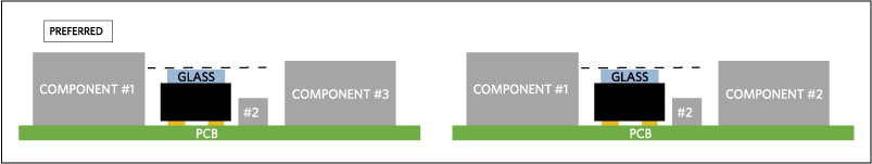
Figure 2. Board layout recommendation.
Stencil Design
Stencil thickness and pattern geometry determine the precise volume of solder paste deposited onto the device land pattern. Stencil alignment accuracy, as well as consistent solder volume transfer, are critical for uniform solder reflow. Stencils are usually made of stainless steel.
- Recommended stencil thickness: 100µm
- Stencil Fabrication: laser-cut with electropolish for better release than the regular laser-cut stencil.
- Stencil Aperture: Design stencil opening to be 1 mil (25µm) per side smaller than the PCB pad size.
- Tolerance must be tightly controlled, as it can effectively reduce aperture size.
- Walls of the apertures should be smooth, with rounded corners and a trapezoidal cross-section, which enhances the release of solder paste from the aperture.
- Stencil aperture must meet the industry-standard area ratio of > 0.66.
SMT Assembly
Standard SMT equipment and process are used for OLGA assembly. The process flow is as follows:

Moisture Sensitivity
All Maxim OLGA modules meet MSL3 standard as per JEDEC specification JSTD020D.1. Parts will be shipped in tray or tape-and-reel form. All parts will be baked and dry-packed with desiccants and a humidity indicator card. If the humidity indicator card has turned pink, or if the parts have been exposed to longer than their floor life, subject the packages to bake at 125°C for 48 hours.
All OLGA parts have vent holes for better moisture sensitivity and reliability. Vent holes should not be blocked during or after SMT.
Refer to JEDEC specification J-STD-033C for correct use of moisture/ reflow sensitive surface-mount devices.
Solder Paste
A no-clean, low-residue solder paste is recommended to mount OLGAs in order not to block vent holes with flux residue or introduce foreign material into the package during cleaning. A Type 3 (or finer) solder paste is recommended for 0.5mm pitch printing. Recommend lead-free SAC305 for solder paste. Please follow paste supplier’s recommended stencil clean frequency for respective solder pastes. Nitrogen purge is recommended during solder reflow
Screen Printing
A metal squeeze should be used with 45-60° print angle. It is recommended to do a post-printing solder inspection to check for print quality.
- Print speed: Start with 20mm/sec; can increase the speed as comfortable.
- Apply a pressure of ~10N/mm with the squeeze while printing.
- Snap of distance: 0mm.
Automated Component Pick and Place
A standard pick and place machine with 0.05mm accuracy can be used for placing the OLGA modules on the printed solder. Conventional placement systems can be employed using either the OLGA outline or the position of the leads as a placement guide. Placement guide using position of the leads tends to be more accurate but slower and requires a complex vision processing system. Package outline placement method runs faster but is less accurate. The contract PCB assembler can determine the most acceptable method to be employed for this process. Low mounting speed is recommended to prevent the paste from squeezing out.
Nozzle/vacuum cup suggestion:
- Material: antistatic rubber
- Pick-Up Location: center of the package
- Vacuum: -60kPa to -95kPa
- Gap Between Nozzle and Glass When Picking Up Units: 0.1mm
- Bond force: 1N
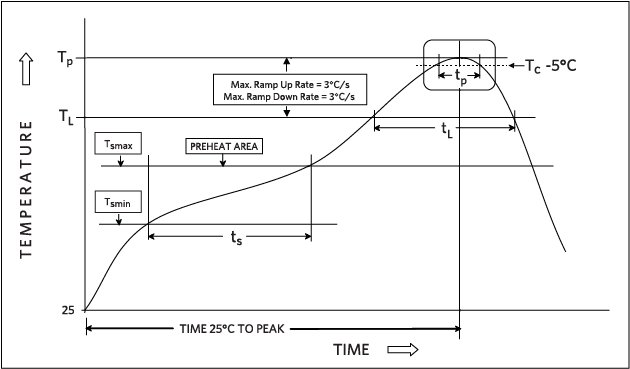
Reflow
Maxim OLGAs are compatible with all industry-standard solder reflow processes. As with all surface-mount devices, it is important that profiles be checked on all new board designs. Additionally, if there are tall components mixed on the board, the profile must be checked at different locations on the board. Component temperatures may vary due to surrounding components, locations of parts on the PCB, and package densities. The reflow profile guidelines are based on the temperature at the actual lead to PCB land pad solder joint location. The actual temperature of the solder joint is often different than the temperature settings in the reflow system.
It is recommended that the profiles be checked using thermocouples at the actual solder joint locations prior to being used for the actual board interconnection reflow.
A forced convection oven with nitrogen, having a temperature uniformity within ±5°C is recommended.
Vent holes should NOT be blocked by solder or flux during or after reflow.
Slow ramp-down rate is preferred to minimize stress in package.
| Profile Feature | Description | Pb-Free assembly |
| Recommendation | ||
| TSmin | Min Soak Temperature | 150°C |
| TSmax | Max Soak Temperature | 200°C |
| ts | Time Between TSMIN and TSMAX | 60–120 Seconds |
| TL | Liquidous Temperature | 217°C |
| tL | Time Above TL | 60–150 Seconds |
| Tp | Peak Package Body Temperature | 260°C |
| tp | Time Witdin 5°C of TP | 30 Seconds |
| Ramp-Up Rate (TL to TP) | 3°C/Seconds (max) | |
| Ramp-Down Rate (TP to TL) | 3°C/Seconds (max) | |
| Ramp-Down Rate (TL to Room Temperature) | 3°C/Seconds (max) | |
| Time 25°C to Peak Temperature | 8 Minutes (max) | |
Flux Cleaning
Cleaning is not recommended as water and foreign material can flood into package through vent holes and cause damage.
Rework
Rework is not recommended. It should only be performed using a controlled and qualified process that prevents mechanical and ESD damage.
Joint Inspection
X-ray can be used to inspect if all the joints are formed successfully. Fewer voids are preferred for better drop test reliability. Void of < 30% joint area is recommended.
Glass Defect
For OLGA packages with glass lids, units with the following defects will be rejected.
- "Close-ended" glass defect:
- Definition: Defect starting and ending at any two sides of the glass lid.
- Reject criteria: Defect line crossing LCP opening if dimension (a or b) is greater than 15 mil.
- "Open-ended" glass defect:
- Definition: Defect starting from one side of glass lid.
- Reject criteria: Any evidence of such defect.
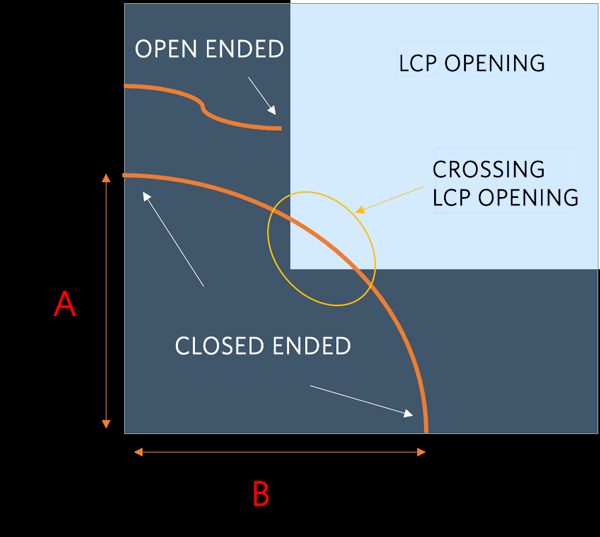
Figure 3. Glass defect criteria.