Modes of Operation on the MAX9949 and MAX9950 Parametric Measurement Units
Abstract
This application note explains the four main operating modes for the MAX9949/MAX9950 parametric measuring units (PMUs). The operating modes are: forced current/measure current (FIMI), forced current/measure voltage (FIMV), forced voltage/measure current (FVMI), and forced voltage/measure voltage (FVMV). Block diagrams, equations, and tables make it easy to verify a sample setup.
Introduction
The MAX9949/MAX9950 are dual-channel parametric measuring units (PMUs) that have four main operating modes:
- FIMI—Forced Current/Measure Current
- FIMV—Forced Current/Measure Voltage
- FVMI—Forced Voltage/Measure Current
- FVMV—Forced Voltage/Measure Voltage
Two other subordinate measurement modes of operation will not be discussed in this note: force nothing/measure voltage (FNMV) and force nothing/measure current (FNMI). For more information on these operational modes, refer to the data sheet.
This application note will explain the four main operational modes in topical sections. Each section shows an equivalent block diagram to illustrate how the function is performed in the silicon. Equations explain the operation; sample setups are presented. A table for the FIMI mode gives further examples and shows how the MAX9949/MAX9950 can be set up for different ADC connections to the MSR pin. The reader can use these examples, setups, equations, and tables to help set up a particular operational mode.
To understand how each mode can be set up with a serial interface, please consult the data sheet.
Caveats and Assumptions
A number of items should be understood before proceeding to the block diagrams.
- This note supplements the information in the data sheet. The reader is advised to have a copy of the data sheet available. This will ensure that all settings remain within specification.
- The examples shown here assume a calibrated setup. For simplicity, all offsets are assumed to be zero. As this is an ideal setup and never the case in a real setting, all offsets need to be calibrated to obtain absolute accuracy.
- Full-scale range (FSR) in the specification refers to the full range from the negative minimum to the positive maximum setting. For example, the 200µA range has an operating FSR of ±200µA = 400µA total range. This is the case for all the other ranges: ±2µA, ±2mA, and ±64mA.
- The linearity error is always expressed as a function of FSR, and is normally within ±0.02%. If we pick the 2µA range, then the maximum linearity error is 0.02% of 4µA = 80nA over the full 4µA FSR.
- Do not exceed the ABSOLUTE MAXIMUM RATINGS. Always operate within the normal operating ranges specified in the data sheet. Operating outside the normal range can lead to erroneous setups and/or damage the part.
- The numbers shown in the ellipses on the drawings are nodal voltages. The reader can follow each node and verify its expected values. The diagrams are actual spice models with ideal op amps; the node voltages are back annotated from the simulation run.
- In the FI (force-current) modes, note that the forced current is proportional to [VIN - VIOS].
- The examples in the tables demonstrate how to set the IOS to accommodate unipolar and bipolar ADCs.
- The example diagrams all use a load of 15.5kΩ. The range was also set to 200µA, by setting RSENSE = 10kΩ. The diagrams are applicable to any load and any range.
- This application note is also applicable to the MAX9951/MAX9952 PMUs with two notable exceptions: the gain multiplier in the feedback loop is four and not two; the sense resistors are doubled. The actual results remain exactly the same.
FIMI Mode

Figure 1. Equivalent block diagram of FIMI mode with sample setup.
The following observations can be made from Figure 1.
- The MSR pin is monitoring the voltage at the IN input pin, plus or minus any offsets from U1, U2, U3, U4, and U5. By itself, the MSR pin is not monitoring the forced current directly. Instead the IFORCE current is directly related to VIN - VIOS by the following formula:
- Figure 1 shows an example of a setup where IN = 3.456V, IOS = 1.234V, and the load = 15.5kΩ. Using Equation 1 and RSENSE = 10kΩ (±200µA range), we see that IFORCE = 111.1µA.
- We can confirm this calculation for IFORCE by calculating the current through RSENSE. Therefore, as expected:

IRSENSE = (2.833 - 1.722)/10,000 = 111.1µA
Finally, at the load:
IRLOAD = 1.722/15,500 = 111.0968µA (Error is due to 3 digits of resolution.)
| FIMI | ||||
| IN (V) |
IOS (V) |
RSENSE (Ω) |
FI (µA) |
MSR (V) |
| IOS set for -4V to +4V ADC on MSR output | ||||
| -4 | 0 | 10,000 | -200 | -4 |
| -3 | 0 | 10,000 | -150 | -3 |
| -2 | 0 | 10,000 | -100 | -2 |
| -1 | 0 | 10,000 | -50 | -1 |
| 0 | 0 | 10,000 | 0 | 0 |
| 1 | 0 | 10,000 | 50 | 1 |
| 2 | 0 | 10,000 | 100 | 2 |
| 3 | 0 | 10,000 | 150 | 3 |
| 4 | 0 | 10,000 | 200 | 4 |
| IOS set for 0V to +8V ADC on MSR output | ||||
| 0 | 4 | 10,000 | -200 | 0 |
| 1 | 4 | 10,000 | -150 | 1 |
| 2 | 4 | 10,000 | -100 | 2 |
| 3 | 4 | 10,000 | -50 | 3 |
| 4 | 4 | 10,000 | 0 | 4 |
| 5 | 4 | 10,000 | 50 | 5 |
| 6 | 4 | 10,000 | 100 | 6 |
| 7 | 4 | 10,000 | 150 | 7 |
| 8 | 4 | 10,000 | 200 | 8 |
Table 1 demonstrates how to use the IOS pin to allow the use of a unipolar ADC (in this case, -4V to +4V) or a bipolar ADC (0V to 8V). Thus, customers can choose from a wide range of ADCs for their application. The example in Table 1 represents the 200µA range (RSENSE = 10kΩ), but the same setup applies for all ranges.
FIMV Mode

Figure 2. Equivalent block diagram of FIMV mode with sample setup.
The FIMV node is basically the same setup as the FIMI mode, but now the voltage at the output or the force pin is monitored with the MSR pin (Figure 2). The forced current is exactly the same as in Figure 1, so all calculations remain the same.
FVMI Mode
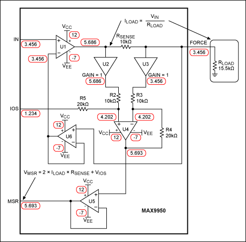
Figure 3. Equivalent block diagram of FVMI mode with sample setup.
In the FVMI mode the loop is set up to force the force pin to the voltage at the IN pin (Figure 3). Therefore, VFORCE = VIN.
This is easily seen in Figure 3 where:
ILOAD = VIN/RLOAD = 3.456/15,500 = 222.97µA
We are in the 200µA range because RSENSE = 10kΩ. Therefore, we are exceeding the FSR of the 200µA range by 22.97µA. This is actually acceptable, because each range will have margin that extends past the FSR specification. Note that the MSR pin is offset by IOS and VMSR = 2 × (ILOAD × RSENSE) + VIOS.
FVMV Mode

Figure 4. Equivalent block diagram of FVMV mode with sample setup.
Figure 4 shows a simple loop where the force output is set to the IN voltage and the MSR pin simply monitors this set or forced voltage. Therefore, ILOAD = VIN/RLOAD.
Summary
This application note elaborated on the data sheet description of the four main operating modes of the MAX9949/MAX9950 PMU devices. The equivalent block diagram for each mode was shown along with a sample setup that can be easily verified.