Low Power Polling with Analog Devices Secure NFC Microcontrollers
Abstract
Modern payment systems are increasingly mobile, and therefore, power is at a premium. Contactless payment technology requires significant power to energize the operational volume and power any payment cards presented to it. This application note presents ideas to significantly reduce the power requirements for payment systems using Analog Devices Secure NFC Microcontrollers. These methods are detailed with plots which show the current usage for each on an actual system. Application code is also provided.
Introduction
The explosion in use of mobile smart phones and their continually expanding capabilities has changed the world of payment. Beyond customers desiring to pay for goods with their phone, retailers, and service provides must be able to accept payments in new and usual places, food trucks, at houses, or even on the side of a highway. Like all battery powered devices, the amount of time these mobile payment systems can operate between charges is a constant challenge.
In direct opposition to long runtimes, Contactless (NFC) payment technology requires significant power to energize the operating volume powering any cards (PICCs) or mobile phones in the field. In recent years, changes to the EMV contactless specification further increased the required power, while modern compact designs reduce antenna size and increase RF loading on the field.
This power, while significant, is only one demand on the battery of the system. Processors, LCDs, wireless communications (Wi-Fi, Bluetooth, Cellular), thermal receipt printers etc., all compete for their portion of the battery's power. Heating is another important consideration of high-power usage, mobile systems are typically sealed tightly to help protect them from environmental concerns and can only dissipate heat through their frames and cases.
This application note considers methods to reduce the power demand for the Contactless interface on Analog Devices' Secure NFC Microcontrollers.
Low Power Polling
Many Point of Sale (POS) terminals are fixed in a location and are always connected to a power source. These systems often use full-speed application polling as power is unlimited, but for mobile payment systems power usage is critical. Mobile systems must consider all the power demands of the system. However, this application note only considers the NFC interface.
Polling Basics
Polling is the procedure by which the NFC reader finds cards in its operating volume. In a typical example, the reader activates the field, then must wait 5.1ms for cards present to power up. After this a wake-up command (WUPA) is sent for Type A cards, then after another 5.1ms, a wake-up command (WUPB) for Type B is sent. Assuming no cards respond to these commands, the reader shuts down the field. Overall, this process takes ~11.2ms. Figure 1 shows the basic polling process.

Figure 1. Basic Polling.
Current Consumption
Since the NFC is not always active, the average power usage is the critical metric. The basic formula for power is:
P = IV
V (Voltage) can be considered fixed here, so there is a direct relationship of I (Current) to power consumption. Figure 2 shows a simplistic view of current used while polling.
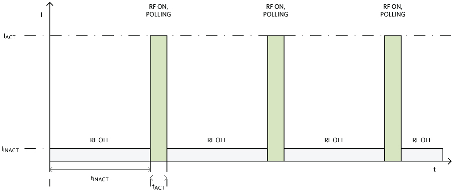
Figure 2. Polling Power Consumption Cycle.
There are two states; Active (Polling) and Inactive (Powered Down). To calculate the average current used while polling compare the duty cycle when the field is active to when it is inactive. Obviously, more active time means higher current consumption. This can be calculated using:

Typical Operating Currents
The Contactless interface has several different power domains or rails:
- Digital: Digital Base Band (DBB), Registers, state machines etc. powered via VMAIN
- Analog Receive: Analog-to-digital Converters (ADCs), Mixer etc. powered via VDD_RF_RX and VDD_RF_1V
- Analog Transmit: Power amplifier etc. powered via VDD_RF_TX
The transmitter consumes the most power by far, with a typical active operating current of 365mA at 3.3V or 1.2 Watts. The actual current consumed by the transmitter is different for every system, as the external connections through the EMC filter, antenna matching circuit and, finally, the antenna are unique for every system. Similarly, external loads near the antenna, such as large metallic parts can increase the load perceived by the transmitted field.
This application note only considers the transmit rail and its associated power. When not actively transmitting, the power consumed for all Contactless supplies in power down mode is the data sheet parameter: IDDA_RF_PD 4.4µA typical. However, current on the transmit rail is effectively zero when not transmitting, so assume there is no power usage when the field is not energized.
Concept of Low Power Polling
The overall reduction of power used during polling comes from minimizing active transmission time. The longer the system goes without field transmission the less power it uses. However, if the system delays excessively, it impacts customer experience. The system should not feel slow to customers. Ideally, low power polling must strike a balance between minimizing power consumption and preserving reasonable customer experience.
This application note covers two mechanisms to reduce the active polling time:
- Reducing the polling rate.
- Reducing the time to detect a card in the field.
Another method which may be used by the system to reduce polling power consumption is to only enable polling when a payment is expected. For instance, polling may be activated only after the seller inputs the sales amount into the POS and hands the device to the paying customer. It can also be disabled if an alternate payment interface is activated first, contact card or magnetic stripe etc. This method is application specific and is beyond the scope of this application note.
Reduction of Polling Rate
Polling less often is the most obvious way to reduce power consumption. All that is required is to add a programmable delay between sequential polling attempts. Recall that standard polling requires ~11.2ms followed by an NFC reset lasting ~5.1ms before repeating the sequence.
Instead of continually polling, after a polling attempt in which no cards are detected, the POS can simply disable the field, and delay or sleep for an extended period. The longer this inactive time the lower the average polling power consumed. However, as previously discussed, the system should not excessively delay as this impacts the customer experience negatively.
For this application note, an inter-polling delay of 400ms is chosen, as a good compromise between power savings and customer experience. This value is a starting point the payment application can and should tune as part of the overall system optimization. For example, a system might be willing to endure longer time between polling attempts to save even more power, at the cost of forcing customers to hold their card in place longer.
Reduction of Card Detection Time
This method is more complex and should be used in conjunction with the reduced polling rate. The idea is to detect potential cards in the field without spending the full ~11.2ms of EMV polling time. If a potential card is detected by this method, the reader proceeds with standard activation to determine whether it is an actual payment card or not. If no potential card is detected, the field is disabled as soon as possible.
To accomplish this, Analog Devices' Secure NFC Microcontrollers utilize the field detection (FD) feature. When actively transmitting this feature samples the field and determines its approximate level. This can be done in much less time than waiting for the required power up time and sending the WUPA/WUPB commands. When a card enters the operating volume of the reader, it reduces the field level slightly as its antenna etc. begin to harvest power from the field. The load a card typically places on the field increases the closer the card is to the antenna.
Different cards present different loads on the field. Some may only reduce the field by a couple FD least significant bits (LSBs). To maximize the sensitivity of the FD feature, during the antenna matching phase of the system design care must be taken to properly set the receiver divider resistor and perhaps adjust the receiver attenuation. The goal is to have the measured FD level when the field is empty to be as close to the maximum value of 255 as possible without exceeding it.
Note: if the field level presented to the receiver is too large, it may always report 255 as the FD level regardless of the load of cards in the field.
Furthermore, if the field measures a low value such as 100 when empty, it provides much less detection sensitivity, and potential cards may not be detected at all or only when very close to the readers antenna. For more details, refer to the PCD Antenna Matching Guide and the AFE Tuning Guide.
For this to work, first the field must be sampled to determine the empty field level. For this application note, this is done by sampling the field 5 times when the example is first activated, and the field level is averaged and recorded.
Subsequent card detection attempts activate the field measuring the current FD level. If the current field is ever lower than the recorded empty field level, it indicates a potential card in the field and full activation proceeds.
The procedure:
- Establish the empty field FD threshold, as described above.
- After the inter-polling delay, activate the reader's RF field. The RF driver routine used for this also initializes the peripheral and performs various calibration procedures.
- Measure the FD level.
- Deactivate the RF field.
- Compare the measured FD level to the empty threshold, if the measured level is less then proceed with the full EMV polling procedure to activate and operate on the potential card.
- Begin inter-polling delay and return to step 2 or cease polling depending on application requirements.
Application vs EMV Certification Polling
It is important to be aware that the polling method required for EMV Level 1 testing is different from the polling which should be used in applications. The polling routine required is specified by EMV's device test environment (DTE) specification to satisfy test tool requirements. Specifically, the certification polling does not issue a reset if no cards are found in the field. It simply sends another round of WUPA and WUPB commands without an interleaved reset.
Note: An NFC reset procedure completely disables the field for 5.1ms, long enough for cards present to lose power and power-on reset (POR).
Certification polling only resets the field if an issue, such as collision etc. is detected, or if indicated by the test machine itself. Application polling resets the field if no cards are detected. Therefore, certification polling uses the highest power of all.
Device Self-Heating
Activating the RF field can consume significant power, sourcing up to 1.2W or more depending on system configuration. Although the transmitter impedance is small, channeling more than an Amp causes the device to self-heat. As the device heats up, the transistors powering the field become less efficient resulting in a slightly reduced field strength. It is recommended to duty cycle the field on and off to alleviate this self-heating.
Device heat dissipation from the secure microcontrollers may be further hampered by system security requirements placing the device inside of a secure mesh or enclosure.
Even using a basic low power polling reduces any issues due to self-heating. However, EMV certification testing requires the highest power polling. If the field remains on for too long, the heat may result in slightly reduced field strength. Testing failures might occur if there is insufficient margin on field strength. Overall, it is highly recommended that during EMV certification, the field is disabled when no tests are actively being performed, and, if necessary, pause testing and disable the field periodically to allow the device to cool.
Thermal Parameters
The thermal resistance (θJA) for the die area near the NFC transmitter is slightly higher than that detailed for the 169-pin ball grid array (BGA) package in the data sheet at 21°C/W vs 18.75°C/W. Prediction of junction temperature is dependent on how much power is being dissipated. Recall that:
TJ = TA + (θJA × PD)
Where TJ is the junction temperature, TA is the ambient temperature, and PD is the power being dissipated in the package. Therefore, the power dissipated directly determines the junction temperature. The power is provided by the VDD_RF_TX rail at 3.3V. The current consumed depends on several variables such as external antenna matching, selected drive strength and operational duty cycle. Transmit drive strength is selected by the final application software, but it is typically the maximum drive possible. Operational duty cycle has been discussed previously and has a direct linear relationship to the power dissipated i.e., if only active for 25% of the time, there is only 25% as much power dissipated and 25% temperature increase. Care should be taken to guarantee that the device does not exceed the absolute max junction temperature of 125°C for any significant amount of time.
External Antenna Matching
The impedance of the external EMC filter, the matching network and the PCD antenna are important factors in the power dissipated by the transmitter. Figure 3 shows a simplified overview of the input impedance (RIN) seen by the transmitter drivers.

Figure 3. Input Impedance seen by Transmit Driver.
Note: RIN is a complex impedance and is determined by all components in the network including resistors, capacitors, inductors, and the antenna coil.
The impedance should be measured using a network analyzer at 13.56MHz. Ideally, this impedance should be measured when installed in the final system assembly as conductive materials nearby can affect the results. For more details, refer to the PCD Antenna Matching Guide.
After determining RIN, the current consumption may be estimated using the following equation determined as a fit line of the data shown in Figure 4.
ITX = 754.95 × RIN−0.513

Figure 4. Impedance vs Transmit Supply Current.
Power Usage Comparison
The following plots show the current usage of the VDD_RF_TX rail during various polling procedures. Table 1 shows a comparison of the power used by each. These current plots were captured by using a Keithley DMM7510 multimeter and plotted using a python script. Each plot uses a different version of card detection which can be seen visually. After a card is found, the application begins full activation (WUPA, ANTICOLLISION, SELECT, RATS) and finally sends a proximity payment system environment application protocol data unit (PPSE APDU). From the response application protocol data units (RAPDU) response, the application identifier code (AID) is retrieved. Some cards include a string of the card name as well, but if not, the AID is looked up from a table of known card types. In each plot, several polling attempts are shown without finding a card followed by a full activation sequence and PPSE APDU exchange.
EMV L1 Certification Polling
Figure 5 shows the polling used during EMV L1 Certification.
Note: No cards are found by the first 2 sequences of WUPA and WUPB, but the third WUPA gets a valid response.
This begins the activation sequence and the AID retrieval. Interestingly, it is even possible to see the card (PICC) response after these commands, as the much smaller changes in the current. After the completion of the PPSE, the card is RESET.
Note: This sequence is just for demonstration purposes, actual payment sequences include several more APDU exchanges and likely a removal process at the end.

Figure 5. EMV L1 Certification Polling with Command Labels.
Constant Polling
This polling variation constantly polls for cards entering the field. However, compared to certification polling, after no cards are found, the field is reset. Figure 6 shows the current usage where the detection period can be identified, that is the time between two activations of the field. Recall the activation requirements of field on for 5.1ms, then WUPA, another 5.1ms delay then WUPB. After no response to either, the field is reset for 5.1ms. The period of detection is 17.6ms with an inactive time of 5.1ms. This represents an active field duty cycle of 71% vs 100% for certification polling.

Figure 6. Constant Polling.
Basic Low Power Polling
Here we reduce the polling rate of the system to reduce power consumption. Polling proceeds in the same way as in the previous example. However, instead of issuing a reset of 5.1ms after no cards are found, the field is deactivated. While the field is disabled, the application delays or sleeps for 400ms before repeating the sequence. 400ms is a good compromise between reading responsiveness and substantial power savings. Figure 7 shows the current plot of this polling scheme. This obviously uses much less power than constant polling. The detection period is increased from 17.6ms to 412ms, but the inactive time increases from 5.1ms to 400ms. This represents an active field duty cycle of 2.9% vs 71% for constant polling.

Figure 7. Basic Low Power Polling.
Field-Level Card Detection
This method expands on the power savings provided by the previous method by reducing the amount of active field time required to detect a card. Instead of using the full ~11.2ms polling sequence, it only actives the field long enough to measure the field level. If the level is below the detection threshold, it begins the normal polling sequence to process the card. For more details on this method, see the Reduction of Card Detection Time section. Using this method, the system only needs to activate the field for 657us, a massive improvement (17x) compared to standard polling time of 11.2ms. This represents an active field duty cycle of only 0.16% vs 2.9% for basic low power polling. To reduce this active field time further, future versions of the RF driver may provide a dedicated card sensing routine. Figure 8 shows the field-level card detection.

Figure 8. Field-Level Card Detection.
Conclusion
The results summarized in Table 1 clearly show the power savings provided by these low-power polling methods. Some systems and applications may not need to minimize power usage, but all should consider the impact that polling duty cycle has on the overall system thermal budget.
Furthermore, the developer can easily modify the detection period to provide the power savings and responsiveness required.
Note: The final table entry which doubles the inactive time for the Field Level Detection method, linearly reduces the average current by half.
| Polling Description | TINACT (ms) | TACT (ms) | IAVG (mA) |
|---|---|---|---|
| EMV L1 Certification Polling | 0 | 12.437 | 365 |
| EMV Constant Polling | 5.164 | 12.437 | 257.9 |
| Basic Low Power Polling (400ms) | 400.026 | 11.952 | 10.6 |
| Field Level Detection Polling (400ms) | 399.736 | 0.657 | 0.603 |
| Field Level Detection Polling (800ms extrapolated) | 799.736 | 0.657 | 0.304 |
Application Code
Application example code which shows the low power polling techniques is included in the most recent Contactless Support Package release as part of the NFC DTE example.