Estimating Switching Speed for the DS2715 NiMH Battery Charger
Abstract
The switching speed of the DS2715 battery charger varies based on charge mode, inductor selection, and battery voltage. In some cases, the speed under various conditions should be known to account for noise sensitivity, peak-to-peak charge current, and inductor selection constraints. This application note provides an easy-to-use spreadsheet for estimating a circuit's switching speed with different component values, battery parameters, and charge modes.
Introduction
When designing with the DS2715 battery charger in switch mode, it is useful to quickly determine the range of frequencies within which the circuit can be expected to transition. Knowing and controlling the switching frequency can help optimize inductor selection, give guidelines for transistor selection, and dictate PCB layout considerations, among other things. Through the different stages of NiMH charging with the DS2715, the varying current-source demands and battery cell voltages alter the frequency of operation over a wide range. This application note presents an analysis of the DS2715 switch-mode circuit, along with an easy-to-use spreadsheet for estimating the switching frequency at various operating points.
Circuit Overview
Figure 1 shows the equivalent circuit for a buck switching charger with a battery and current-sense resistor as a load. The DS2715 operates by regulating the voltage across RSENSE to a preset value. The sense resistor value, along with this preset reference voltage, then controls the value of ICHARGE. For NiMH batteries, four stages of charging are preferred—three of which (Precharge, Fast-Charge, and Topoff) are regulated through the voltage across the sense resistor. The fourth stage, Maintenance, replenishes the self-discharge of the cells with a small continuous charge current through a nonregulated path. The precharge and topoff states operate at 25% of the average current regulated during fast-charge. This is accomplished in the DS2715 by adjusting the internal reference voltage for VSENSE to reduce ICHARGE.
The various charge states are entered depending on the state of the battery stack. When the battery voltage is less than 1.0V, precharge mode is used to slowly charge depleted batteries. Fast-charge mode is only used when the battery voltage is above 1.0V and not more than 1.65V, but may also terminate when other fast-charge conditions are met. Topoff mode follows fast-charge mode for a preset period of time. RPARASITIC is an optional parameter that has been added to the reference circuit to represent any significant parasitic voltage drops that may occur as a result of battery, fuse, or other connection nonidealities.

Figure 1. The DS2715 switching reference circuit.
The control circuit for regulating the sense resistor voltage consists of a comparator with hysteresis and a reference voltage, which drives an open-drain output pin. The hysteresis of the precharge and topoff modes is approximately 25% of the fast-charge value due to the smaller reference voltage used in those modes. Switching speed is determined by the amount of time needed for ICHARGE to go from one peak to the other and back again, which includes any delays in the feedback circuit and in the process of turning QSW and DCATCH off and on. These delays cause ICHARGE to overshoot one or both of the comparator thresholds, creating a larger peak-to-peak variation than nominal. Figure 2 shows an example of ideal switching control waveforms, while Figure 3 shows waveforms with extra turn-off delays in QSW.
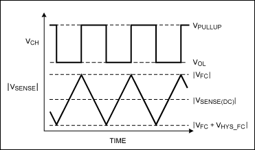
Figure 2. Ideal charge-current control waveforms. (Not drawn to scale.)

Figure 3. Charge-current control waveforms with slow QSW turn-off. (Not drawn to scale.)
Calculation Method
The rate of change for ICHARGE is governed by the voltage and current relationship of an ideal inductor L.
V = L × di/dt and dt = L × di/V
Hence, the amount of time for the on and off states of QSW varies with the voltage developed across L in each state, and the change in ICHARGE from peak to peak. The peak-to-peak value of ICHARGE is set by the hysteresis value of the charge mode and any control circuit delays that cause overshoot of the comparator levels. See the DS2715 data sheet for definitions of the sense comparator fast-charge reference voltage (VFC) and the hysteresis voltage (VHYS_FC).
In order to simplify the switching-speed approximation, let us make the assumption that the voltage across the inductor for each QSW state stays constant. Let us also assume that the midpoint of VSENSE from peak to peak [VFC + (0.5 × VHYS_FC)] provides a reasonable steady-state condition for calculating the inductor voltage of each state. With those simplifications in place, the voltage drop around the loop of the reference circuit in Figure 1 for the QSW_ON and QSW_OFF states can be calculated to yield the inductor voltage for a given battery voltage as follows:
VL(QSW_ON) = VIN - VDIODE - VQSW - VPAR - VBATT - VSENSE
VL(QSW_OFF) = VPAR + VBATT + VSENSE + VDCATCH
Since the battery voltage may vary over a 1.0V to 1.65V range in fast-charge mode, it is useful to calculate the inductor voltage and then the switching speed at several operating points. A spreadsheet is available for download that will perform the calculations described in this application note for three different battery voltages in fast-charge mode, and at one battery stack voltage in precharge and topoff modes.
Once the inductor voltages for each state and each operating point are calculated, any delays in the control circuit may be factored into the on and off times for QSW. For our approximation, this is accomplished by first calculating the extra change in ICHARGE due to the turn-on and turn-off delays of QSW according to the following formulas:
di(on delay) = dt × V(on)/L, where dt = tPDLY + tSW_OFF
di(off delay) = dt × V(off)/L, where dt = tPDLY + tSW_ON
This extra change in current can be thought of as ICHARGE overshooting the comparator threshold due to the control signal or transistor switching delay. Here again for simplicity, we have assumed that the inductor voltage stays constant during each state. When the extra di due to delays is added to the theoretical current change due to hysteresis, we have:
di(Qsw_ON) = VHYS_FC/RSENSE + di(on delay)
di(Qsw_OFF) = VHYS_FC/RSENSE + di(off delay)
This adjusted delta ICHARGE is substituted into the ideal inductor equation, along with the previously calculated inductor voltage, to determine the overall QSW on and off state times. Typically, bipolar circuits are the most likely to contribute enough switching delay to require this extra level of delay consideration, but the delays may be modeled by the user for MOSFET circuits as well.
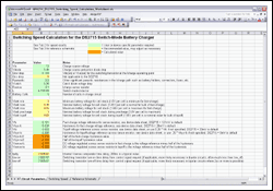
The equations described in this application note have been implemented in a spreadsheet for easily estimating the switching speed of a DS2715 switch-mode charger circuit. The spreadsheet describes each of the parameters that must be entered by the user, or that may be optionally modified by the user (Figure 4).
More detailed image (PDF, 132kB)
Figure 4. Switching-speed calculation spreadsheet.
The first set of parameters relates to the component properties of the reference schematic. The second section contains the various operating points of the battery stack used in the calculations. The third section describes the internal set points of the current-sense comparator; the default values in this section should be verified from the data sheet of the DS2715. Finally, the last section of parameters is for the delays inherent to the DS2715 and any extra delays induced by the switching circuit that must be considered for accurate estimation.
Calculation Results
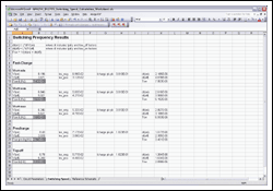
After entering the parameters for the application circuit into the first tab of the accompanying spreadsheet, the results of the switching calculations can be viewed in the second tab (Figure 5). This tab shows the results for each mode and battery operating condition, as well as some of the partial calculations that are used in the final switching-speed result. Included among these are the inductor voltages for each state, the change in ICHARGE due to delays, and the individual on and off state times.
More detailed image (PDF, 123kB)
Figure 5. The switching-speed results tab.
Conclusions
Many useful pieces of information can be taken from the estimations of switching speed as they relate to the reference circuit. It can be seen that the main factors affecting the switching speed of the DS2715 switch-mode NiMH charger are the inductor value, ICHARGE, the headroom of VIN above the battery stack voltage, and in some cases delays resulting from the slow switching of QSW. The analysis presented here can be used to estimate switching speed for these circuits and develop an understanding for how best to adjust this speed when necessary.