Enhanced RSSI Calibration for APDs Using the DS1864
Abstract
This application note explains how to use the DS1864 SFP laser and diagnostic IC to perform enhanced receive signal strength indicator (RSSI) calibration for optical receivers that use an avalanche photodiode (APD). The article discusses the relationship between APD and RSSI, and describes the principal operation of enhanced RSSI on the DS1864.
APD RSSI Overview
Many optical modules use avalanche photodiode-based (APD) optical receivers for high-sensitivity applications. In such modules, receive signal strength indicator (RSSI) is based on the optical photocurrent, rather than electrical signal amplitude at the output of the transimpedance amplifier (TIA). Figure 1 shows a typical current-monitor circuit with a voltage output.
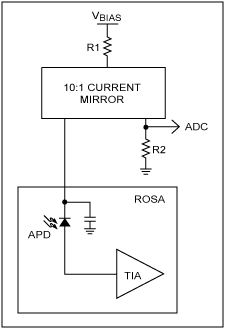
Figure 1. Schematic for a typical APD current monitor.
The current through the APD is given by the equation IAPD = PRX × M × η where:
IAPD is current in mA
PRX is received power in mW
M is the APD avalanche gain factor
η is the conversion efficiency in A/W
Conversion efficiency depends on many structural factors, temperature, and wavelength; it is typically between 0.65 < η < 0.95.
APD gain is achieved by biasing the APD near its breakdown voltage, VBR, which is typically between 20V and 80V and dependent on both the APD structure and operating temperature. The closer the APD is biased to its specific breakdown voltage, the higher is M. While the APD is in avalanche mode, the M is proportional to VBR and VAP, the voltage applied to the APD, as shown in the relationship of
VADV = IAPD × (1/10) × R2 = PRX × M × η × (1/10) × R2
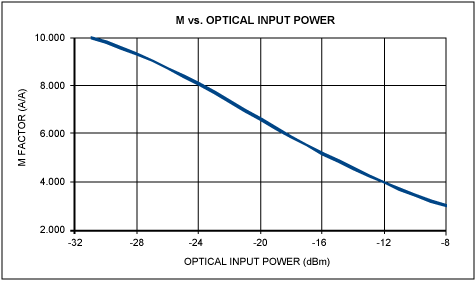
Figure 2. A typical APD gain curve.
Enhanced RSSI Overview
The DS1864 SFP laser and diagnostic IC includes an enhanced RSSI mode for the MON3 channel, which is a differential input to the 13-bit ADC. Enhanced RSSI is also known as dual-range functionality. In enhanced RSSI mode, the ADC takes up to two different readings, called fine and course modes. (Pages 20 and 21 of the DS1864 data sheet describe this mode.) The fine reading is automatically used to measure small input signals. If a large signal is input to the ADC, however, the course mode is automatically used.
For APD RSSI measurements, it is important to note that the two ranges of enhanced RSSI have independent offset and scale calibration factors. Further, the fine mode also allows for up to 7 right shifts of the ADC result. When configured for 7 right shifts, the maximum fine mode reading is 01FFh, and the minimum course mode reading is 01E0h. There are 31 bits of hysteresis to prevent the two ranges from toggling in the overlapping region (01FFh to 01E0h).
Dual-Range Calibration for APD RSSI
To comply with SFF-8472, the monitor circuit and ADC must be calibrated so that one LSB = 0.1µW. Because M varies with input power, the optimal ADC step size must vary to maintain each LSB at 0.1µW. If M varies from 3 to 10 and a single ADC LSB weight is used, this will yield a total error of
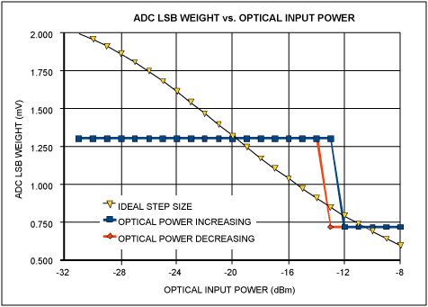
Figure 3. A typical APD monitor's the ideal ADC LSB weight and actual calibrated weights.
The crossover between the LSB weights occurs between ADC step 1E0h and 1FFh when the MON3 fine conversion is configured for 7 right shifts. The optimum LSB weight values must be determined based on the APD and monitor circuit. The resulting RSSI error given this previous example is shown in Figure 4.
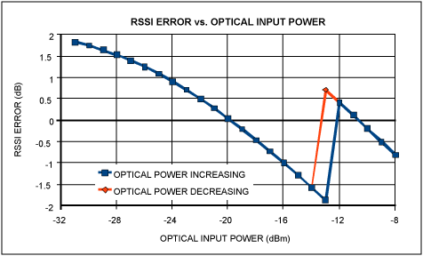
Figure 4. RSSI error in a typical APD monitor application.