Circuit Converts PWM to Amplified and Buffered Linear Signal
Abstract
A simple circuit converts a low-voltage PWM signal to an amplified and buffered linear output. Intended for fan speed control, it allows a 3.3V input to provide linear control of a 12V fan.
Analog Devices makes a variety of fan speed controllers with PWM outputs to control fan speed as a function of temperature. These work by cycling the power to the fan off and on. The fan's speed with the duty cycle setting the fan's speed. In many situations the typical application circuit for these is adequate. However, some situation require a constant power supply to the fan due to audible noise from the fan modulation.
If the noise from cycling the fan's power is too much, consider the circuit of Figure 1. In this case, complementary pair of BJTs (Q1) and a PMOS FET (Q2) create a linear amplifier.
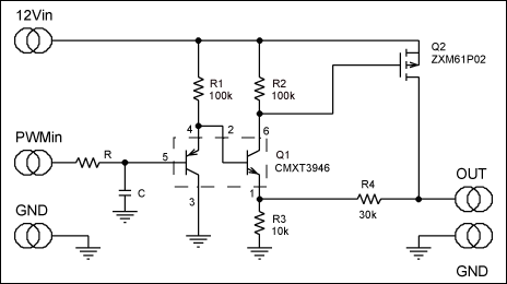
Figure 1. A simple circuit converts a low-voltage PWM signal to an amplified and buffered linear output.
The circuit works in the following manner. The base of the PNP in Q1 is the non-inverting input to the amplifier, and the emitter of the NPN is the inverting input. The PNP is biased as an emitter follower, and the NPN is used both as an emitter follower and as the initial gain element. As the PNP and the NPN operate at roughly the same current density and temperature, the two input voltages approximately track each other. Any current which flows out of the inverting input is mirrored to the NPN collector, causing a drop across resistor R2. The drop across R2 drives the VGS of Q2, which is amplified at Q2's drain, the amplifier output. The output rises to voltage sufficient to null the inverting input to approximately zero current, at which point the amplifier has reached a stable operating point.
The amplifier as specified has about 100mV of output offset primarily due to the burden of forcing the drop across R3 to the VGS threshold of Q2. This is inconsequential given the target application of fan speed control. The amplifier is configured with a gain of +4, which is suitable for taking a 3.3V PWM signal and level shifting up to a 12V maximum output swing when the PWM signal approaches 100% duty cycle.
A CMXT3946 was selected for Q1 due to its dual complementary structure, but this could be substituted with discrete transistors with virtually no degradation in performance. A ZXM61P02 PMOS FET is a good choice for most single fans, and its 800mW max power dissipation allows it to drive fans up 133mA at 6V outputs. Because most fans act approximately resistively, a fan with a peak current of 250mA or less at 12V should be acceptable. Of course, the fan should be measured across its operating range to ensure the power dissipation is within the PMOS FET's specification. If driving multiple fans or high-current fans, an SOIC MOSFET should be substituted for the SOT23 device shown.
The circuit as shown does not have values for the input filter. Select a cutoff frequency, 1 / [6.28 * R * C] at least two decades below the PWM frequency to reduce the PWM ripple at the output. A resistor value as high as 100kΩ is acceptable due to the high input impedance of the circuit.