TD-SCDMA Reference Design V1.0
Abstract
This application note presents Maxim's TD-SCDMA reference design V1.0. TD-SCDMA is the Chinese Third Generation (3G) standard. China's government has allocated 3 frequency bands: 1880~1920MHz, 2010~2025MHz, and 2300~2400MHz. Maxim's TD-SCDMA reference design 1.0 focuses on the 2015~2025MHz band, which is the first frequency band for TD-SCDMA. Included are the block diagram, test results, PCB layout outlines and measured performance.
Additional Information:
- Wireless Product Line Page
- Quick View Data Sheet for the MAX2306, MAX2308, MAX2309
- Quick View Data Sheet for the MAX2361, MAX2363, MAX2365
- Quick View Data Sheet for the MAX2470, MAX2471
- Applications Technical Support
Introduction
TD-SCDMA (time division synchronous code division multiple access) is one of three 3G standards. The Chinese government recently (2002-10) allocated 155MHz of bandwidth for this standard. The TD-SCDMA standard now has three frequency bands: 1880~1920MHz, 2010~2025MHz, and 2300~2400MHz. Maxim currently produces many RF ICs that will operate in these frequency bands, and support the new standard, as is evidenced by the performance documented here.
This document presents the performance of Maxim's TD-SCDMA V1.0 (version one) reference design, and discusses the design specification and testing results. The full performance specification for the radio is documented by 3GPP (Third Generation Partnership Project) (www.3gpp.org) in specification 25.945 V5.0.0.
TD-SCDMA Reference Design Description
The Maxim TD-SCDMA reference design Version 1.0 is a single-mode, single-band transceiver intended to support the TD-SCDMA standard. All active ICs in this reference design are from Maxim, except one PLL required due to fast lock-time requirements. This transceiver operates from a single 2.9V to 3.6V supply, drawing about 73mA in receive mode and about 373mA in transmit mode, while delivering +16dBm at antenna port. This reference design offers a complete handset transceiver design, providing the highest integration available in the industry.
The complete radio is designed to fit a single-sided 40mm x 65mm PCB. The radio transceiver block diagram is shown in Figure 1. This transceiver is designed to meet the TD-SCDMA handset radio specification, 3GPP TR 25.945 (sections 5.1-5.3), "RF Requirements of 1.28Mcpc UTRA TDD Option."

Figure 1. TD-SCDMA RF transceiver block diagram.
The interface board block diagram is shown in Figure 2. This board serves as a convenient test tool for evaluating the radio. All logic I/O and registers are programmed via the DB25 PC parallel port connector, the DIP-switch block and jumpers. Potentiometers provide variable AGC voltages, and buffers provide single-ended baseband I/O through SMA connectors (differential I/Q TX is available via jumper selection). For radio testing without a mature baseband processor, the interface board includes adjustable baseband filters at the I/Q inputs and outputs. The interface board also provides a connector in the lower left-hand region for attaching a programmable logic device to operate the transceiver at full speed. In this way dynamic mode switching can be observed in real time.

Figure 2. Interface board block diagram.
Figure 3 is a photo of the radio mounted on the interface board; Figure 4 identifies the location of the major blocks of the radio, as well as the PCB dimensions.

Figure 3. TD-SCDMA on interface board.

Figure 4. TD-SCDMA transceiver dimensions.
Key Specification Summary
PLL and Frequency Stability
All test data were taken at room temperature, ~25°C
| No. | Parameter | Symbol | Test Condition | Technical Specs/Ref. Subcluse | 3Gpp Spec. | We Measure | Our Target | Units |
| 1 | Frequency stability | Fsb | TR 25.945/5.2.3 | ±0.1 | ±0.015 | ±0.05 | PPM | |
| 2 | RF PLL phase noise | Φn | Set RF LO at 1.75GHz | -83 1KHz offset -87 5KHz offset -89 10KHz offset -98 50KHz offset -110 100KHz offset |
-80 -82 -83 -95 -110 |
dBc/Hz | ||
| 3 | Integrated phase noise of RF PLL | Θrms | Over 1kHz ~ 1MHz | 0.5 | < 1 | DEG | ||
| 4 | RF PLL lock time | Tlock | Final frequency error < 40kHz | 120 | 80* | < 120 | µS | |
| 5 | IF PLL phase noise | Φn | Set IF LO at 528MHz | -88.5 1KHz offset -93.5 5KHz offset -94.3 10KHz offset -110 50KHz offset -122 100KHz offset |
-82 -87 -88 -104 -120 |
dBc/Hz | ||
| 6 | Integrated phase noise of IF PLL | Θrms | Over 1kHz ~ 1MHz | 0.24 | 0.5 | DEG | ||
| Note*: The final frequency error we use is 40kHz, but the standard request is that the frequency should be within ±7kHz after 120µS. | ||||||||
Receive Measurement vs. Target Performance
All test data were taken at room temperature, ~25°C
| No. | Parameter | Symbol | Test Condition | Technical Specs/Ref. Subcluse | 3Gpp Spec. | We Measure | Our Target | Units |
| 1 | RF input frequency range | Frf | TS 25.102/5.2 | 2010~2025 | 2010~2025 | 2010~2025 | MHz | |
| 2 | Noise Figure | NF | To meet the sensitivity level at –108dbm.1.28MHz with 2dB design margin | TR 25.945/5.3.3.3 | 9 | 9 | 9 | dB |
| 3 | Gain control range | Gcr | With -17dBm output swing level to 50Ω load | TR 25.945/5.3.3 TR 25.945/5.3.4 | 80 | 95 | 95 | dB |
| 4 | Front-end 3rd-order input intercept point | IIP3_8MHz | Gain is 3dB below maximum gain, main RF channel is 2010MHz, two CW interference located in 2018.2MHz and 2026.2MHz with the power level: -30dBm | TR 25.945/5.3.8 | -17 | -4.2 (High gain LNA) | -5 | dBm |
| 5 | Front-end 2rd-order input intercept point | IIP2 | Gain is 3dB below maximum gain, main RF channel is 2025MHz, one CW interference located in 1893.6MHz with the power level: -20dBm | TR 25.945/5.3.7 | 16 | 54.7 | 50 | dBm |
| 6 | Channel 3rd-order input intercept point | IIP3_ch | -60dBm input | TR 25.945/5.3.4 (Note 1) | -33 | -35 | dBm | |
| -50dBm input | -25 | -25 | ||||||
| -25dBm input | -7 | 0 | ||||||
| 7 | Adjacent channel selectivity | ACS | ACS at +1.6MHz | TR 25.945/5.3.5 | 33 | 28 (Note 2) | 33 | dBc |
| 8 | Spurious Response | Spr | LO 1747.8MHz Interference: 2044.76MHz, -44dBm Test I/Q noise floor increment | TR 25.945/5.3.7 | <3 | 1.55 | <3 | dB |
| 9 | Spurious Emission | Spe | 9K~1MHz Res:100KHz |
TR 25.945/5.3.9 | -57 | -94 | -80 | dBm |
| 1G~2.01GHz Res:1MHz | -47 | -85 | -80 | |||||
| 2.01G~2.17G Res:1MHz | -64 | -91.8 | -80 | |||||
| 2.17G~12.75G Res:1MHz | -47 | -86.7 | -80 | |||||
| 10 | Block 1dB compression point | PB1dB | Gain is 3dB below maximum gain, main RF channel is 2017.2MHz, one CW interference located in 2013.8MHz | TR 25.945/5.3.6.1 | > -55 | -40.2 | > -45 | dBm |
| 11 | In-band Blocking | Pbin | @ -3.2M offset | TR 25.945/5.3.6.1 | -61 | -61 | -61 | dB |
| @ +3.2M offset | -61 | -61 | -61 | |||||
| @ -4.8M offset | -49 | -49 | -49 | |||||
| @ +4.8M offset | -49 | -49 | -49 | |||||
| 12 | Out-of-band Blocking | Pbout | Fw 2010M, Fuw 2005.2M | TR 25.945/5.3.6.1 | -44 | -44 | -44 | dB |
| Fw 2025M, Fuw 2029.8M | -44 | -44 | -44 | |||||
| Fw 2025M, Fuw 2095M | -30 | -30 (Note 3) | -30 | |||||
| Note 1: TR 25.945/5.3.4 request the maximum input power is -25dBm, we think the input 3rd-order input intercept point should be higher than this power level, consider 18dB, so we think that the input 3rd-order specification should be -7dBm. Note 2: The SAW filter in this design is not adequate; we will replace it with an improved SAW filter in the future to meet this specification. Note 3: Out-of-band blocking at 2095MHz is not met because of the poor rejection of the RF band pass filter. Replacing this filter with at least 10dB rejection at 2095MHz will resolve this problem. |
||||||||
Transmit Measurement vs. Target Performance
All test data were taken at room temperature, ~25°C
| No. | Parameter | Symbol | Test Condition | Technical Specs/Ref. Subcluse | 3Gpp Spec. | We Measure | Our Target | Units |
| 1 | RF frequency range | Frfout | TS 25.102/5.2 | 2010~2025 | 2010~2025 | 2010~2025 | MHz | |
| 2 | Maximum output power | Pout_max | Measured with RRC filter response with a roll off α = 0.22, BW = 1.28M | TR 25.945/5.2.2 | +24 for Class 2 +21 for Class 3 |
+25.3 | +24 | dBm |
| 3 | Minimum output power | Pout_min | Measured with RRC filter response with a roll off α = 0.22, BW = 1.28M | TR 25.945/5.2.4.3 | -49 | -64 | -55 | dBm |
| 4 | Transmit OFF power | Pout_off | Measured with RRC filter response with a roll off α = 0.22, BW = 1.28M | TR 25.945/5.2.5.1 | -65 | < -78 (Note 1) | -96 | dBm |
| 5 | Turn on time | Ton | Use a Function waveform generator to control TxON pin | TR 25.945/5.2.5.2 | 10 | 3.3 | < 5 | µS |
| 6 | Occupied bandwidth | BWout | The bandwidth containing 99% of the total integrated power. | TR 25.945/5.2.6.1 | 1.6 | 1.37 | 1.5 | MHz |
| 7 | Spectrum Mask | Sp_mask | Pout = 25dBm, Res: 30K. While the standard only request 21dBm, so we have a big margin | TR 25.945/5.2.6.2.1 | -18.7, 0.8M offset | -21.9 | -20 | dBc |
| -32.7, 1.8M offset | -42.4 | -33 | ||||||
| -47.9, 2.4M offset | -49.2 | -48 | ||||||
| -47.9, 4M offset | -58.2 | -50 | ||||||
| 8 | Adjacent channel leakage power ratio | ACLR | Measured with RRC filter response with a roll off α = 0.22, BW = 1.28M, here Pout = 25dBm Valid: Pach >-55dBm | TR 25.945/5.2.6.2.2 | ACP: 33 | Acpl: -40.7 | ACP: 36 | dBc |
| Acpu: -38.5 | ||||||||
| ALT: 43 | Altl: -52.3 | ALT: 46 | ||||||
| Altu: -57.3 | ||||||||
| 9 | General Spurious Emissions | Spur | 9K~150K Res:1K | TR 25.945/5.2.6.3 | -36 | -67 | -50 | dBm |
| 150K~30M Res:10K | -36 | -81 | -50 | |||||
| 30M~1G Res:100K | -30 | -74 | -50 | |||||
| 1G~2.013G Res:1M | -30 | -39.3 | -35 | |||||
| 10 | Transmit intermodulation | The interference signal: CW, -40dB below output power | TR 25.945/5.2.7.1 | P = 21dBm, offset 1.6M, -31 | Offset 1.6, -41 | -34 | dBc | |
| P = 21dBm, offset 3.2M, -41 | P = 23.8dBm, offset -3.2M, -55 | -44 | ||||||
| Note 1: In our test, -78dBm/1.28MHz is the noise floor of Agilent 8560E, not the real output power. To test this specification, we need a good LNA with the gain greater than 30dB. We estimate if the off power is greater than -96dBm, it will affect the receiver, so our target is -96dBm. | ||||||||
Receiver Tests
All test data were taken at room temperature. Many system related specifications such as sensitivity, intermodulation, blocking, Tx and Rx emissions, spurious response, spectrum mask, and etc., have been measured. The following test results demonstrate that the Maxim TD-SCDMA Reference Design V1.0 is a fully functional TD-SCDMA radio.
Reference Sensitivity and Cascade NF
3GPP TR 25.945 calls for the following sensitivity spec; receiver tests refer to this level as REFSENS. This level assumes the input is a single coded dedicated physical channel (DPCH), as if the base station was transmitting only to the handset under test. Also, it assumes that all the received energy corresponds to the DPCH and not to the pilot channel or any other signaling. At REFSENS, BER (bit error rate) has degraded to 0.001.
| Parameter | Level | Unit |
| ΣDPCH_Ec/Ior | 0 | dB |
|
|
-108 | dBm/1.28MHz |

According to TR 25.945, we know that if we consider 2dB margin, the maximumnoise figure of the receiving path can't be greater than 9dB. So we will use NF (noise figure) to compute the reference sensitivity.
Usually noise figure is measured with Noise Figure Analyzer, but when it comes to the cascaded noise figure measurement, we measure the RF board from antenna input to the I/Q output. Since the frequency of the I/Q output is too low to measure with NF Analyzer, we apply "direct noise measurement" to measure the cascade noise figure.
NoiseFloor = -17dBm + NF + G + 3
If Noise Floor and G are measured, NF can be deduced easily. Refer to Figure 5.

Figure 5. Cascaded NF test.
Test result:
PRFin = -96.1dBm and PIQout = -0.37dBm , so G = 95.7dB
Noise Floor = -66.3dBm/Hz, so NF = 174+ (-66.3) -95.7-3 = 9dB.
Comments:
With gain (95.7dB) set, the RxQ level is about 1.1Vp-p with no input signal.
Test Instrument:
Agilent 8648C Signal Generator
Agilent E4405B Spectrum Analyzer
Gain Control Range
The receiver gain control range is defined with the fixed receiver baseband output voltage swing level. In our measurement, we use the -17.5dBm with 50-Ω load to characterize. In the TD-SCDMA spec TR25.945/5.3.3&4, the required receive gain control range is 80dB. This reference design's receiver has two places to control the cascaded gain; one is the gain step control of the LNA (inside MAX2538), the other is the continuous gain control with IF VGA (inside MAX2309).
- Gain step with LNA: 20.4dB
- Cascade gain varying with the AGC voltage
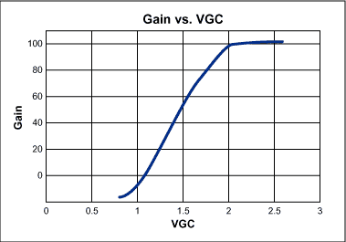
Figure 6. Cascaded receive gain vs. AGC (LNA in gain mode).
Comments:
From above curve, we can see that the gain dynamic range is about 100dB. The gain varies linearly with VGC varying from 2V to 0.9V. Note that if we consider the gain step of LNA, the total gain range is about 120dB.
Test Instrument:
Agilent 8648C Signal Generator
Agilent E4405B Spectrum Analyzer
Front-End IIP3 Test
The front-end IIP3, (input third order intercept) includes the LNA and mixer. From the test procedure below, one notes that the difference between input CW signal and RFLO is greater than IF. In this condition, the IF SAW filter will provide large suppression for these mixed signals, so the back end circuitry makes no contribution to nonlinearity.
Two CW signals at 2018.2MHz and 2026.2MHz are input, utilizing a signal combiner at the antenna. Due to the nonlinearity of the LNA and RF Mixer, there should be a 3rd order inter-modulation product in-band (RFLO = 1747MHZ, IFLO = 526MHz). Observe it with the spectrum analyzer at 200kHz. This test should be carried out with specified VGC (gain control voltage) and gain settings.
Refer to the following calculating procedure:
IM3(dBc) = Pout - Pout_IM3
IIP3 = Pin + IM3 / 2 And refer to test setup, Figure 7.

Figure 7. IIP3 test set up.
Test Result:
A: LNA in high gain
Test condition: VGC = 1.5V, Gain = 55dB, LO = 1747MHz
PRF1 = -30dBm @ 2018.2MHz, PRF2 = -30dBm @ 2026.2MHz
Calculation: Pout_IM3 = -48dBm @ 200kHz
IM3= (-20 + 34) - (-48) = 62dBc
IIP3 = -20 + IM3/2 = +11dBm
B: LNA in low gain
Test condition: VGC = 1.5V, Gain = 34dB, LO = 1747MHz
PRF1 = 20dBm @ 2018.2MHz, PRF2 = -20dBm @ 2026.2MHz
Calculation: Pout_IM3 = -48dBm @ 200kHz
IM3 = (-20 + 34) - (-48) = 62dBc
IIP3 = -20 + IM3 / 2 = +11dBm
Test Instruments:
Agilent E4405B Spectrum Analyzer
Agilent 8648c Signal Generator
Agilent E4432B Signal Generator
Front-End IIP2 (Half IF Offset Response)
Apply an RF CW signal at 1893.6MHz to the antenna port. Due to the nonlinearity of LNA and RF Mixer, there will be a 2nd inter-modulation signal falling into the receive band. Observe this signal at 200kHz with the spectrum analyzer. The measured IM2 is usually called the half-IF offset interference. So the input RF signal frequency is (1762 + 263/2 + 0.1 = 1893.6MHz).See Figure 8 for test setup.
Refer to the following calculating procedure:
IM2(dBc) = Pout - Pout_IM2
IIP2 = Pin + IM2

Figure 8. IIP2 test.
IIP2 Test:
Test condition: AGC = 1.5V, Gain = 55dB, LO = 1762MHz
PRFin = -20dBm @ 1893.6MHz
Calculation: Pout_IM2 = -39.7dBm @ 200kHz
IM2 = (-20 + 55) - (-39.7) = +74.7dBc
IIP2 = -20 + 74.7 = +54.7dBm
Comments:
Based on above test results, we can calculate if half IF response can meet spurious response requirement:
PRFin = -44dBm
IIP2 = 54.7dBm
Pin_IM2 = PRFin - (IIP2 - PRFin) = -142.7dBm, it's far below channel white noise power at room temperature, so there is no problem with this specification.
Half IF Offset Response Test:
Here we test the half IF offset response directly to verify if it can meet the standard request. We consider half IF response as a special response frequency point, and according to 3GPP standard, we know if the changing of channel noise power of Rx Q or Rx I not greater than 3dB, it is acceptable.
Test Condition:
LO = 1762MHz, RF power = -44dBm, RF frequency = 1893.6MHz, AGC=1.96V

Figure 9. No RF input.

Figure 10. With RF input.
Comments:
From the two photos above, we find that the BB Noise Δis only 0.11dB, so there is no problem with the half IF offset response performance.
Test Instruments:
Agilent E4405B Spectrum Analyzer
Agilent E4432B Signal Generator
Channel IIP3 Test and Maximum Input Level
Channel IIP3 Test:
Here we want to know the nonlinearity character for the entire receive path. We use two in-band CW signals at the antenna port, and test the inter-modulation result from the I or Q output port. In this reference design, we use the MAX2309 as the IF VGA and I/Q demodulator. According to the MAX2309's data sheet, the IIP3 of MAX2309 varies with the gain as shown in Figure 11, so we know the channel IIP3 will vary with the input signal level. Below we will give two test results with different input signal levels while keeping the output I and Q signal levels constant. Also given is the budget calculation result.

Figure 11. The IIP3 of MAX2309 varies with the gain of MAX2309.
Test Method:
Apply two RF signals of 2010.3MHz and 2010.4MHz at the antenna. Observe the I/Q output port. There should exist two inter-modulation signals at 200kHz and 500kHz. Select the maximum magnitude of the two 3rd inter-modulation signals and the minimum magnitude of the two output main signals to calculate the IM3. Please refer to Figure 7 for test set-up details.
Test Result:
Test condition 1:
LO = 1747MHz, IFLO = 526MHz
PRF1 = -50dBm @ 2010.3MHz, PRF2 = -50dBm @ 2010.4MHz
AGC = 1.381V, Gain = 37.9dB
Result:
IIP3 = -12.3 + (-12.3 - (-63) ) / 2 - Gain ≈ -25dBm

Figure 12. Channel IIP3 test, input signal level is -50dBm.
Test condition 2:
LO = 1747MHz, IFLO = 526MHz
PRF1 = -60dBm @ 2010.3MHz, PRF2 = -60dBm @ 2010.4MHz
AGC = 1.47V, Gain = 49.5dB
Result:
IIP3 = -10.6 + (-10.6 - (-64.2) ) / 2 - 49.5 ≈ -33dBm

Figure 13. Cascade IIP3 test, input signal level is -60dBm.
Budget calculating result is shown in Figure 14:

Figure 14. Cascade IIP3 vs. input signal strength.
From the above curve, (Figure 14) one sees that the test result is very close to the calculated result. Figure 14 shows a computed curve where we set two switching points at -40dBm and -45dBm. As the input signal increases, when it equals -40dBm, the MAX2538 is set to the low gain mode. As the input signal decays in amplitude, the MAX2538 is set to the high gain mode when the input level equals -45dBm. This gain-switching method provides 5dB of hysteresis.
Test Instrument:
Agilent E4405B Spectrum Analyzer
Agilent 8648c Signal Generator
Agilent E4432B Signal Generator
Maximum Input Level:
This is defined as the maximum receiver input power at the UE (user equipment)antenna port which does not degrade the specified BER performance. Belowis the minimum requirement specified by TR 25.945:
| Parameter | Level | Unit |
| ΣDPCH_Ec/Ior | -7 | dB |
|
|
-25 | dBm/1.28MHz |
Comments:
From the RF budget calculation (refer to Figure 14 ), one finds the input cascade IIP3 is about -5dBm when the input power is -25dBm. This provides adequate linearity for proper operation with the maximum signal.
Adjacent Channel Selectivity (ACS)
Adjacent Channel Selectivity is a measurement of a receiver's ability to detect a wanted signal at its assigned channel frequency in the presence of an adjacent channel signal. ACS is the ratio of the receive filter attenuation on the assigned channel frequency to the receiver filter attenuation on the adjacent channel. Additional suppression of the unwanted signal is provided by the baseband filters.
For this test, the desired signal is a modulated test signal at -91dBm. The jammer is a modulated signal at the upper adjacent channel (+1.6MHz offset) at -53dBm (+38dBc). The test is done with no additional suppression provided by the baseband I/Q filters.
The output spectrums with and without additional adjacent channel suppression are shown in Figures 15a and 15b. With the baseband filters, ACS improves 4 to 5dB. Since total power measurements were not taken on the spectrum analyzer, estimations of total integrated channel powers are made.

Figure 15a. Baseband output spectrum from ACS test (no baseband filtering)
Total integrated power of the desired signal is approximately +1dBm, and total integrated power of the unwanted signal is approximately +8dBm. ACS is the difference between the two (+7), adjusted for the original +38dBc; ACS is approx 28 dB.

Figure 15b. Baseband output spectrum from ACS test (with base band filtering). Note adjacent channel is suppressed an additional 4 to 5dB.
| Specification | Requirement | Test Result |
| ACS at +1.6MHz | 33dB | 28dB |
Test Instruments:
R/S FSEA30
Intermodulation Test
Third and higher order mixing of the two interfering RF signals can produce an interfering signal in the band of the desired channel. Intermodulation response rejection is a measure of the capability of the receiver to receive a wanted signal on its assigned channel frequency in the presence of two or more interfering signals which have a specific frequency relationship to the wanted signal.
The relative increase in the base band noise floor is measured to determine whether or not the radio passes this test.
Receive AGC voltage is set for minimum sensitivity level. The total system gain is 95.8dB.
The following steps describe the test method for testing intermodulation:
- With no RF input, measure the baseband noise floor (in a 1.28MHz bandwidth). Figure 16 shows this result.
- (For the high side intermodulation product) Input a CW signal at 2020.2MHz and a modulated signal at 2023.4MHz. Each signal is -46dBm. Calculate the rise in the baseband noise floor. See Figure 17.
- (For the low side intermodulation product) Input a CW signal at 2013.8MHz and a modulated signal at 2010.6MHz. Each signal is -46dBm. Calculate the rise in the baseband noise floor. See Figure 18.
Note: The RF LO = 1754MHz, so RF main channel is at 2017MHz.

Figure 16. Baseband noise floor with No RF input.
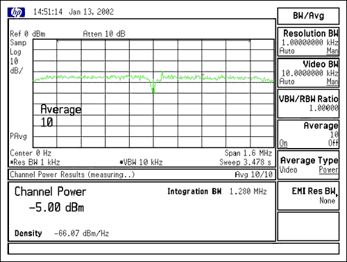
Figure 17. High-side intermodulation test.

Figure 18. Low-side intermodulation test.
| fmain_channel (MHz) |
funwanted1 (CW, MHz) |
funwanted2 (dBm/1.28MHz) |
Interferer
Power (each) (dBm) |
BB
Noise Floor (dBm/MHz) |
BB
Noise Δ (dB) |
| 2017 | 2020.2 | 2023.4 | -46 | -5.00 | +1.40 |
| 2017 | 2013.8 | 2010.6 | -46 | -5.08 | +1.32 |
With no RF input, the baseband noise floor is -6.40dBm/1.28MHz
Comment:
Intermodulation tests pass.
Test Instruments:
Agilent E4405B, Spectrum Analyzer
Agilent 8648C, Signal Generator
Agilent E4432B, Signal Generator
Blocking
Two types of blocking test are required:
- Blocking 1dB compression point.
- Normal blocking test based on the TD-SCDMA standard
Blocking 1dB Compression Point:
When a receiver detects a very weak signal in the presence of a strong interference, there will exist two kinds of degradation: noise floor rising and gain compression.
To test blocking 1dB compression level, apply the desired CW signal, PRF1 = -106dBm at 2017.2MHz. An interfering CW signal PRF2 at 2013.8MHz is also applied through a combiner. Then adjust the interfering signal's power and record the power of the interfering signal when the desired signal is compressed 1dB. Note that the RFLO is 1754MHz, IFLO is 526MHz here. The test set up is shown in Figure 7.
Test Result:
PRXQ = -11.1dBm @ 200kHz
When PRF2 = -40.2dBm, PRXQ is compressed 1dB.
Test Instrument:
Agilent E4405B Spectrum Analyzer
Agilent 8648c Signal Generator
Agilent E4432B Signal Generator
Normal Blocking Specification Test:
Blocking characteristics are a measure of the receiver's ability to detect a desired signal at its assigned channel frequency in the presence of an unwanted interferer without this unwanted input signal causing a degradation of the performance of the receiver beyond a specified limit. 3GPP TR 25.945 defines this limit at BER = 0.001 maximum. The blocking performance shall apply at all frequencies except those at which a spurious response occur. A relaxed blocking spec is applied to these spurious frequencies.
Since the REFSENS specification is defined in the absence of blockers, the blocking and spurious specs are met when the base band noise floor rises by less than the allowed increase of the wanted signal (+3dB). Without the ability to measure BER, blocking and spurious performance are shown to meet the specified limit where the baseband noise floor is increases by less than 3dB when subjected to the blocker.
The following steps describe the test method for testing in-band and out-of-band blocking:
- With no input signal, measure the base band noise floor.
- (In-band blocking) Input a modulated signal at the power and frequencyd offset specified below. The specification is met if the noise floor rises by less than 3dB.
- (Out-of-band blocking) Tune the radio and input a CW signal as in the table below. The specification is met if the noise floor raises by less than 3dB.

Figure 19. Base band spectrum with on-channel modulated signal at REFSENS+3dB, no blocker.
| Frequency Offset (MHz) |
Interferer Power (dBm/1.28MHz) |
BB
Noise Floor (dBm/1.28MHz) |
>BB
Noise Δ (dB) |
| - | (no interferer) | -6.51 | 0 |
| -3.2 | -61 | -6.07 | +0.44 |
| +3.2 | -61 | -6.40 | +0.11 |
| -4.8 | -49 | -6.26 | +0.25 |
| +4.8 | -49 | -6.26 | +0.25 |
| funwanted (MHz) |
fwanted (MHz) |
Interferer
Power (dBm/1.28MHz) |
BB
Noise Floor (dBm/1.28MHz) |
BB
Noise Δ (dB) |
| 2005.2 | 2010.0 | -44 | -4.45 | +2.06 |
| 2029.8 | 2025.0 | -44 | -4.51 | +2.00 |
| 2095.0 | 2025.0 | -30 | +3.96 | +10.47 |
The radio passes all in-band blocking tests. Out-of-band blocking at 2095MHz is not met because of the poor rejection of the RF band pass filter (see Figure 20). Replacing this filter with an improved on offering at least 10dB rejection at 2095 will allow this specification to be met.
Test Instruments:
Agilent E4405B Spectrum Analyzer
Agilent E4432B Signal Generator

Figure 20. S11 and S21 of RF BPF. Note the 2dBto 3dB rejection for 2095MHz blockers.
Spurious Response
Spurious response is a measure of the receiver's ability to detect a desired signal on its assigned channel frequency without exceeding a given degradation due to the presence of an unwanted CW interfering signal at any other frequency at which a response is obtained (i.e., for which the blocking limit is not met). Spurious responses are defined by the following equation:
fIF = mfRF + nfLO (Where m and n can be < or > zero.)
The relative increase in the base band noise floor is measured to determine whether or not the radio passes the spurious response test (see Blocking section).
Spurious Response Requirements and Test Results
With no RF input, the baseband noise floor is -6.02dBm/1.28MHz
| fLO (MHz) |
funwanted
(CW, MHz) |
Interferer
Power (dBm) |
m | n | BB
Noise Floor (dBm/MHz) |
BB
Noise Δ (dB) |
| 1747.8 | 2035.1 | -44 | 7 | -8 | -4.24 | 1.78 |
| 1747.8 | 2119.1 | -44 | -4 | 5 | -5.44 | 0.58 |
| 1747.8 | 2044.76 | -44 | -5 | 6 | -4.47 | 1.55 |
With no RF input, the base band noise floor is -5.07dBm/1.28MHz
| fLO (MHz) |
funwanted
(CW, MHz) |
Interferer
Power (dBm) |
m | n | BB
Noise Floor (dBm/MHz) |
BB
Noise Δ (dB) |
| 1747.8 | 2083 | -44 | 6 | -7 | -3.49 | 1.78 |
| 1747.8 | 1995.2 | -44 | -6 | 7 | -4.97 | 0.1 |
Comments:
Spurious response tests pass.
Test Instrument:
Agilent E4405B Spectrum Analyzer
Agilent E4432B Signal Generator
Spurious Emissions
The Spurious Emissions Power is the power of emissions in a receiver that appear at the antenna connector.
Spurious Requirements and Test Results
Test condition: LO = 1754MHz
| Band | Spurious Emissions Measured | Spurious Emissions Allowed |
| 9kHz - 1000MHz | <-94dBm/100KHz | -57dBm/100KHz |
| 1000MHz - 2010MHz | <-85dBm/1MHz | -47dBm/1MHz |
| 2010MHz - 2170MHz | <-91.8dBm/1MHz | -64dBm/1MHz |
| 2170MHz - 12.75GHz | <-86.72dBm/MHz | -47dBm/1MHz |
| RF LO Leakage | <-88dBm |
Comments:
Spurious tests pass.
Test Instrument:
Agilent E4405B Spectrum Analyzer
I/Q Gain/Phase Imbalance
There are two printed circuit boards comprising Maxim's TD-SCDMA reference design. One is the RF transceiver board, and the other is the interface board. There are receiver baseband active filters on interface board. I/Q gain and phase imbalance are specified before and after these filters.
Test Method:
Apply an RF CW signal at the antenna port and measure the I and Q signal from two places as discussed above, compare signal's voltage and phase difference with oscilloscope. The RF signal generator is adjusted to produce baseband frequencies of 300kHz and 500kHz.
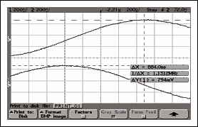
Figure 21. After LPF phase imbalance test @300kHz.

Figure 22. Before LPF phase imbalance test @300kHz.

Figure 23. Before LPF phase imbalance test @500kHz.
From Figures 21, 22 and 23 above:
| RxI Amp. (mVpp) |
RxQ Amp. (mVpp) |
Amp.
Imbalance (mv) |
Phase Imbalance | |
| After LPF@300kHz | 680 | 670 | 10 | 5.5° |
| Before LPF@300kHz | 563 | 575 | 12 | 1.8° |
| Before LPF@500kHz | 625 | 625 | 0 | 3.9° |
Test Instrument:
Agilent 8648C Signal Generator
Agilent 54622D OSCILLOSCOPE
Transmitter Tests
The following TX tests are covered:
- Output power dynamic range
- Transmitter-off power
- On-time test
- Output RF spectrum emissions
- Transmit intermodulation
Output Power Dynamic Range
For the handset, the maximum output power should be +24dBm at the antenna port for a class 2 handset, +21dBm for class 3 handset, and the minimum output power should be less -49dBm. In Maxim's TD-SCDMA reference design, MAX2363 is the key device for meeting this requirement. This TX IC provides about a 90dB dynamic range. Here we use two methods to set the gain of MAX2363. Both the AGC voltage is adjusted, and the control registers in the MAX2363 are used to shutdown the PA driver stage of MAX2363, and provide attenuation for the signal path. The attenuation is about 25dB. The test setup is depicted in Figure 24.

Figure 24. Output power test setup.
Test Instrument:
Agilent E4405B Spectrum Analyzer
Agilent E4432B Signal Generator
Test Condition:
I/Q input signal= 70mVrms (12%)
Vbat = 3.4V
Operation control register of MAX2363 = 9FEFH
Configuration register of MAX2363 = 143FH
Current control register of MAX2363 = 2C74H
Test Result:
| Pout (dBm) | AGC (V) | IFG | Zero_bias | I_mult | Itotal
(mA) Includes interface board |
|
| 25.3 | 2.6 | 111 | 0 | 0100 | 785 | |
| 24 | 2.44 | 111 | 0 | 0100 | 735 | |
| 19.5 | 2.3 | 111 | 0 | 0100 | 521 | |
| 16.3 | 2.25 | 111 | 0 | 0100 | 437 | |
| 13.2 | 2.2 | 111 | 0 | 0100 | 384 | |
| 9.2 | 2.15 | 111 | 0 | 0100 | 351 | |
| 5.1 | 2..1 | 111 | 0 | 0100 | 333 | |
| 1.6 | 2.05 | 111 | 0 | 0100 | 327 | |
| -1.47 | 2 | 111 | 0 | 0100 | 325 | |
| -3.5 | 2 | 111 | 0 | 0000 | 320 | |
| -6.7 | 1.95 | 111 | 0 | 0000 | 319 | |
| -9.5 | 1.9 | 111 | 0 | 0000 | 318 | |
| -12.6 | 1.85 | 111 | 0 | 0000 | 317 | |
| -16 | 1.8 | 111 | 0 | 0000 | 316 | |
| -19.7 | 1.75 | 111 | 0 | 0000 | 315 | |
| -20.4 | 2.1 | 111 | 1 | 0000 | 316 | |
| -26.6 | 2 | 111 | 1 | 0000 | 313 | |
| -32.6 | 1.9 | 111 | 1 | 0000 | 311 | |
| -39.4 | 1.8 | 111 | 1 | 0000 | 310 | |
| -46.6 | 1.7 | 111 | 1 | 0000 | 309 | |
| -50.8 | 1.65 | 111 | 1 | 0000 | 309 | |
| -55.4 | 1.6 | 111 | 1 | 0000 | 309 | |
| -59.5 | 1.55 | 111 | 1 | 0000 | 309 | |
| -63.9 | 1.5 | 111 | 1 | 0000 | 309 | |
| From above table: - Maximum output power is 25dBm, meeting class 2 (24dBm at antenna port) and class 3 (21dBm at antenna port) handset standards. - Minimum output power is -64dBm. The standard specifies a minimum output power of -49dBm. - The output dynamic range is approximately 90dB |
||||||
Transmitter-Off Power
The transmit OFF power state is when the UE does not transmit. This parameter is defined as the maximum output transmit power within the channel bandwidth when the transmitter is OFF. The requirement for transmit OFF power shall be less than -65dBm measured with a filter that has a Root-Raised Cosine (RRC) filter response with a roll off α = 0.22 and a bandwidth equal to the chip rate.
To test this specification, we connect an Agilent 8560E spectrum analyzer to the antenna connector to test directly. The test result is about -78dBm/1.28MHz. This is far below the required -65dBm, so there is no problem with this specification. We know if the OFF power is -78dBm, it will affect the receiver. Assuming the isolation of T/R switch from Tx to Rx is 20dB, and it is estimated that the OFF power can be below -96dBm, then it's quite ideal. In this test setup, -78dBm/1.28MHz is the noise floor of Agilent 8560E, not the real output power. In order to test this specification, we need a good LNA (low noise amplifier) with gain grater than 30dB.
On TimeTest
Below is the test setup for transmitter ON Time test:

Figure 25. Transmitter ON Time test.
Test Instruments:
Agilent 8560E Spectrum Analyze
Agilent E4432B Signal Generator
Agilent 33120A Function/Arbitrary Waveform Generator
Test Result:
Transmitter on time = 3.25µs is shown in Figure 26. The standard specifies 5µs maximum. Please refer to below photo:

Figure 26. Transmitter on time test screen.
Output RF Spectrum Emissions
This section covers the following tests:
- Occupied bandwidth
- Spectrum emission mask
- Adjacent channel leakage power ratio (ACLR)
- Spurious emissions
Occupied Bandwidth
Occupied bandwidth is a measure of the bandwidth containing 99% of the total integrated power for the transmitted spectrum and is centered on the assigned channel frequency. According to the TD-SCDMA standard, the occupied bandwidth is about 1.6MHz based on a chip rate of 1.28Mcps. Use an Agilent E4405B to test the occupied bandwidth. The test setup is shown in Figure 24.
Test Instruments:
Agilent E4405B Spectrum Analyzer
Agilent E4432B Signal Generator
Test Condition:
I/Q input signal = 12% (70mVrms)
Vbat = 3.4V, AGC = 2.6V, Pout = 25dBm
Operation control register of MAX2363 = 9FEFH
Configuration register of MAX2363 = 143FH
Current control register of MAX2363 = 2C74H
Test Result:
Occupied bandwidth = 1.367MHz, and can meet standard request. The standard request is 1.6MHz. Please refer to below photo:
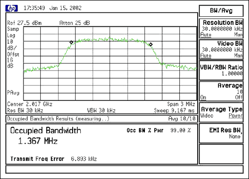
Figure 27. Occupied bandwidth test.
Spectrum Emission Mask
Out-of-band emissions are unwanted emissions immediately outside the nominal channel resulting from the modulation process and non-linearity in the transmitter but excluding spurious emissions. The spectrum emission mask applies to frequencies, which are between 0.8MHz and 4MHz from a carrier frequency. Use a spectrum analyzer to test this specification. Refer to Figure 24 for the test setup.
Test Instruments:
Agilent E4405B Spectrum Analyzer
Agilent E4432B Signal Generator
Test Condition:
I/Q input signal = 12% (70mVrms)
Vbat = 3.4V, AGC = 2.6V, Pout = 25dBm (Standard request 21dBm, so we have big margin)
Operation control register of MAX2363 = 9FEFH
Configuration register of MAX2363 = 143FH
Current control register of MAX2363 = 2C74H
Test Result:
From Figure 36:
| Offset | Suppression | Standard Requirement | Note |
| 0.8MHz | -21.9dBc | -18.7dBc | The resolution used here is 30KHz, and the ratio is external 30KHz power over in-band 30KHz power. |
| 1.8MHz | -42.4dBc | -32.7dBc | |
| 2.4MHz | -49.2dBc | -47.9dBc | |
| 4MHz | -58.2dBc | -47.9dBc |

Figure 28. Spectrum emission mask test.

Figure 29. Spectrum emission mask test result.
Note:
- The blue line is the standard requirement
- Four red points are test results, and all are below the blue line, so there is no problem with this specification.
- Here the channel power is +25dBm; it has four dB margins over the standard request. The standard request is +21dBm.
Adjacent Channel Leakage Power Ratio (ACLR)
Adjacent Channel Leakage power Ratio (ACLR) is the ratio of the transmitted power to the power measured in an adjacent channel. Both the transmitted power and the adjacent channel power are measured with a filter response that has a Root-Raised Cosine (RRC) filter response with roll-off α = 0.22 and a bandwidth equal to the chip rate.
Use an Agilent E4405B spectrum analyzer to test this specification. Set POUT to maximum, for worst-case ACLR. Refer to Figure 24 for the test setup.
Test Instruments:
Agilent E4405B Spectrum Analyzer
Agilent E4432B Signal Generator
Test Conditions:
I/Q input signal = 12% (70mVrms)
Vbat = 3.4V, AGC = 2.6V, Pout = 25dBm
Operation control register of MAX2363 = 9FEFH
Configuration register of MAX2363 = 143FH
Current control register of MAX2363 = 2C74H
Test Result:

Figure 30. Adjacent channel ACLR test.

Figure 31. ALT channel ACLR test.
From Figures 30 and 31:
| POUT | ACPlow | ACPup | ALTlow | ALTup | Standard Requirement | |
| ACP | ALT | |||||
| 25.2dBm | -40.7dBc | -38.5dBc | -52.3dBc | -57.3dBc | -33dBc | -43dBc |
Spurious Emissions
Spurious emissions are emissions which are caused by unwanted transmitter effects such as harmonics emission, parasitic emission, intermodulation products and frequency conversion products, but exclude out of band emissions. It applies to frequencies which are over 4MHz from the center frequency of RF carrier.
According to the Spec. measure the peak power at different frequency band with different RBW by the aid of Spectrum Analyzer. Refer to Figure 24 for the test setup.
Test Instruments:
Agilent E4405B Spectrum Analyzer
Agilent E4432B Signal Generator
Test Conditions:
I/Q input signal = 12% (70mVrms)
Vbat = 3.4V, AGC = 2.6V, Pout = 25dBm, RF frequency = 2017MHz
Operation control register of MAX2363 = 9FEFH
Configuration register of MAX2363 = 143FH
Current control register of MAX2363 = 2C74H
Test Results:
| Frequency Bandwidth (Hz) | Spec. Requirement (dBm) | Measured (dBm) | RBW |
| 9K~150K | -36 | -67 | 1k |
| 150K~30M | -36 | -81 | 10k |
| 30M~1G | -30 | -74 | 100k |
| 1G~2.013G | -30 | -39.3 | 1M |
| 2.050G~3G | -30 | -31 | 1M |
| Other freq. bandwidth | According to the Spec., the spurious emission at 3GHz~12.5GHz should also be tested, but it can't be completed due to the ESA4405B's limitation of frequency. | ||
| Note: Due to the instrument's limitation, we can't measure the spurious at DCS and GSM band as required by 3GPP standard. | |||
Transmit Intermodulation
The transmit intermodulation performance is a measure of the capability of the transmitter to inhibit the generation of signals in its non-linear elements caused by presence of the wanted signal and an interfering signal reaching the transmitter via the antenna.
To test the transmitter intermodulation, a circulator is used. According to TD-SCDMA standard, the transmitted signal should be a modulated signal, but it is difficult distinguish the intermodulation products, so here we use two kinds of signal this characteristic. One signal is CW, while another is modulated signal. For a detailed test setup, please see Figure 32.
Test Instruments:
Agilent E4405B Spectrum Analyzer
Agilent E4432B Signal Generator
Agilent 8648C Signal Generator

Figure 32. Transmitter intermodulation test.
Test Conditions:
I/Q input signal = 12% (70mVrms)
Vbat = 3.4V, RF frequency = 2017MHz
Operation control register of MAX2363 = 9FEFH
Configuration register of MAX2363 = 143FH
Current control register of MAX2363 = 2C74H
Test Results:
| Pwant | Signal Type | Puw (CW)* | Offset | Test Result | Standard | Refer |
| 24dBm | CW | -40dBc | 1.6MHz | -62.5dBc | Figure 33 | |
| 21dBm | CW | -40dBc | 1.6MHz | -65.6dBc | Figure 34 | |
| 21.8dBm | CW | -30dBc | 1.6MHz | -53.3dBc | Figure 35 | |
| 21.3dBm | Modulated | -40dBc | 1.6MHz | -40.9dBc | -31dBc | Figure 36 |
| 23.5dBm | Modulated | -40dBc | -1.6MHz | -39.5dBc | -31dBc | Figure 37 |
| 23.8dBm | Modulated | -40dBc | -3.2MHz | -55.0dBc | -41dBc | Figure 38 |
| *Note that the Puw (power un-wanted) level is tested at the antenna port of TD-SCDMA reference design. Through the test result, you can see that the TD-SCDMA reference can meet the standard request. | ||||||

Figure 33. Transmitter intermodulation test 1.

Figure 34. Transmitter intermodulation test 3.

Figure 35. Transmitter intermodulation test 4.

Figure 36. Transmitter intermodulation test 2.

Figure 37. Transmitter intermodulation test 5.

Figure 38. Transmitter intermodulation test 6.
DC Consumption Test
Test Method:
Test the DC consumption in the states of TX, Rx, Idle, Sleep and Shutdown with using a digital multimeter.
Test Results:
Test condition: Vcc = 3.45V
| Sub Circuit | Test Results | Tx | Rx | Idle | Sleep | Shutdown |
| PLL Part | 16mA |  |
|
|
||
| Receiver | 57mA | |
||||
| Interface Board | 64mA | |||||
| Transmitter (25dBm) | 707mA | |
||||
| Transmitter (24dBm) | 657mA | |
||||
| Transmitter (16dBm) | 357mA | |
| Working Mode | Tx Mode | Rx Mode | Idle | Sleep | Shutdown | ||
| 25dBm | 24dBm | 16dBm | |||||
| Total IDC | 723mA | 673mA | 373mA | 73mA | 16mA | 0mA | 0mA |
| Note: Does not include interface board current. | |||||||
PCB Layer Stackup
In this design, we use 6 layers PCB stackup. Figure 4 gives more detailed information:

Figure 39. PCB layer stackup uses FR-4 dielectric.
Fabrication notes:
- All surface mount components are on the top side (Except the 100 Pin connector).
- All VIAs are through hole.
- Minimum VIA is 18mil diameter with 8mil drill.
- Minimum spacing:
- PAD - PAD: 8mil
- PAD - Track: 8mil
- Track - Track: 8mil
- VIA - VIA: 8mil
- Final board thickness is about 54mil.