MAX16800 Test Board
Abstract
MAX16800 test board is a simple high-brightness LED-driver circuit board developed for driving LEDs made by Osram, Lumileds, Nichia, Cree, and others. The test board demonstrated that the MAX16800 is ideal for automotive interior and exterior LED lighting, and commercial and industrial LED lighting.
General Description
40V, 350mA, Adjustable Linear High-Brightness LED Driver
The MAX16800 test board is a fully assembled and tested circuit for evaluating the MAX16800 high-brightness LEDs driver. The MAX16800's output current is programmed by using an external current-sense resistor in series with the LED. An enable (EN) pin allows a wide range of PWM dimming. The MAX16800 is well-suited for automotive applications requiring high-voltage input and is able to withstand load dump events up to 40V.
Features
- ±3.5% Output Current Accuracy
- Integrated Pass Element with Low-Dropout Voltage (< 1.2V)
- +5V Regulated Output with 4mA Source Capability
- Differential LED Current Sense
- Low Shutdown Supply Current (12mA, typ)
- Low 204mV Current-Sense Reference Reduces Power Losses
- Works Down to +5V for Automotive Cold Cranking
- Wave-Shaped Soft Edges Reduce Radiated EMI During PWM Dimming
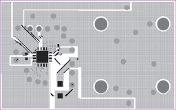
Board Layout and Connection

Specifications
| Input Voltage | 6.5V to 40V |
| LED Current (load Current) | 0.35mA to 350mA, set at 350mA |
| Maximum Output Voltage | Input Voltage—0.6V (typ.) |
| Short-Circuit Protection | Continuous |
| Thermal Shutdown | 155°C (typ) |
| PWM/ENable Pin Voltage | Up to 40V |
| PWM Dimming Range | 100Hz to 1KHz (typ.) |

Actual Size: 2" × 1.25"

PCB Top Silkscreen
PCB Top Layer
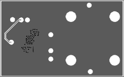
PCB Bottom layer

Schematic Diagram
| Reference | Part | Value | Manufacturer |
| C1 | - | 0.1µ, 50V, 10%, Ceramic X7R, (0603) | - |
| C2 | - | 0.1µ, 10V, 10%, Ceramic X7R, (0402) | - |
| R1 | - | 0.56Ω, 1%, (1206) | - |
| U1 | MAX16800ATE | Linear Adjustable, High-Brightness LED Driver | Maxim |
| LED | Q65110A2922 | Golden DRAGON White LED (LW W5SG) | OSRAM Opto |
| LED* | LXHL-MW1B | Luxeon Star/C White LED | Lumileds |
| *Note: Can drive Luxeon Star LEDs or any other high-brightness LEDs. | |||
Instructions
VIN+: Connect the positive terminal of the DC input source to J1-1.
GND: Connect the negative terminal of the DC input source to J1-2.
LED+: Connect the anode of the LED string to this pad. When external LEDs are used, disconnect the LED that is on the board.
LED-: Connect the cathode of the LED string to this pad. When external LEDs are used, disconnect the LED that is on the board.
PWM/EN: This pin can be used either to enable/disable the LED driver or to apply a PWM dimming signal. Putting a jumper from the VIN+ pin to the PWM/EN pin will turn the LED driver on. To turn the LED driver off, use the jumper to connect the PWM/EN pin to GND.
By applying a PWM signal between the PWM/EN and GND pins, the LED current can be chopped from 0 to 100% of its maximum current setting. Changing the duty cycle of the PWM signal will change the brightness of the LEDs. It is also possible to dim the LEDs by PWM chopping the VIN+ (input supply) while the EN pin is connected to VIN.
LED Current Setting: LED current is set to 350mA. It can be adjusted by changing the value of R1 based on the following equation: ILED = VSENSE / R1.
The current can be modified by adding an external resistor across the LED- and GND pins of J2. Make sure to disconnect R1 when an external resistor is used.
To monitor the current through the LEDs a scope probe can be placed across the J2 pins. The measured voltage divided by the R1 is the same as the current going through the LEDs.
Linear Dimming: The LED current can be adjusted linearly by changing the value of the R1 or by adding an offset voltage to the LED- pin. The offset voltage can be generated by connecting a resistor-divider from V5 REG to the LED- and GND pins.
Open LED: Disconnecting the LEDs while the driver is running will not cause any damage to the LEDs or the driver.
Power Dissipation: Thermal shutdown turns the device off if power dissipation in the IC causes the junction temperature to reach 155°C (typ). An external resistor can be added at the input to the device or in series with LEDs to reduce the power dissipation in the IC. The resistor's power rating should be higher than I²R. (I is the input current or LED current, and R is the value of the added resistor.)
V5: The +5V regulator can be used to power other components from J4. When the EN pin is connected to GND (the device is disabled), the V5 pin turns off to minimize the standby current.
| Jumper | Setting | Effect |
| J2 | Open | R1 senses LED current |
| J2 | Short | Device will internally current-limit to the maximum current set by the short-circuit current limit (800mA, max). This may cause LED damage. |
| J2 | R1-removed; external resistor added to these pins | Current through the LEDs will be determined by the value of resistor on J2. |
| J3 | No jumper | Will cause an undetermined voltage on the EN pin, which can enable or disable operation. |
| J3 | Pins 1 and 2 shorted | Device enabled; LED current regulated. |
| J3 | Pins 2 and 3 shorted | Device disabled; in low-current standby, V5 turns off. |