MAX1452 Serial Communications
Abstract
The MAX1452 utilizes asynchronous serial data communication via a single-pin interface. This application note provides a detailed description of the serial communication system used and should be read in conjunction with the MAX1452 data sheet.
This application note describes the serial communications system used in the MAX1452, and it is best read in conjunction with the MAX1452 data sheet. It expands on the serial communications information contained in the data sheet and provides communication examples.
MAX1452 Digital Mode
The MAX1452 digital input/output (DIO) provides single-pin serial communications with internal control functions and memory. All command inputs flow into a set of 16 registers, which form the interface register set (IRS). Additional levels of command processing are provided by control logic, which takes its inputs from the IRS. A bidirectional 16-bit latch buffers data to and from the 16-bit calibration registers and internal (8-bit-wide) EEPROM locations. Figure 3 shows the relationship between the various serial commands and the MAX1452's internal architecture.
Communication Protocol
The DIO serial interface is used for asynchronous serial data communications between the MAX1452 and a host calibration test system or computer. The MAX1452 automatically detects the baud rate of the host computer when the host transmits the initialization sequence. Baud rates between 4800 and 38,400 can be detected and used. The data format is always 1 start bit, 8 data bits, and 1 stop bit. The 8 data bits are transmitted LSB first, MSB last. A weak pullup can be used to maintain a logic 1 on DIO while the MAX1452 is in digital mode. This is to prevent unintended 1 to 0 transitions on this pin, which would be interpreted as a communication start bit. Communications are allowed only when the Secure-Lock™ byte is disabled (i.e., CL[7:0] = 00HEX) or UNLOCK is held high.
Initialization Sequence
The first command byte sent to the MAX1452 after power-up or following receipt of the re-initialization command is used by the MAX1452 to learn the communication baud rate. The initialization sequence is a 1-byte transmission of 81 hex, as follows:
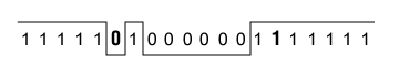
The start bit, shown in bold above, initiates the baud-rate synchronization. The 8 data bits 81 hex (LSB first) follow this and then the stop bit, also shown in bold above. The MAX1452 uses this sequence to calculate the time interval for a 1-bit transmission as a multiple of the period of its internal oscillator. The resulting number of oscillator clock cycles is then stored internally as an 8-bit number (BITCLK). Note that the device's power supply should be stable for a minimum period of 1ms before the initialization sequence is sent. This allows time for the power-on reset function to complete and DIO to be configured by the Secure-Lock byte or UNLOCK.
Re-Initialization Sequence
The MAX1452 provides for re-establishing or relearning the baud rate. The re-initialization sequence is a 1-byte transmission of FF hex, as follows:

When a serial re-initialization sequence is received, the receive logic resets itself to its power-up state and waits for the initialization sequence. The initialization sequence must follow the re-initialization sequence to re-establish the baud rate.
Serial Interface Command Format
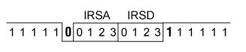
All communication commands into the MAX1452 follow the format of a start bit, 8 command bits (a command byte), and a stop bit. The command byte controls the contents of the interface register set and comprises a 4-bit interface register set address (IRSA) nibble and a 4-bit interface register set data (IRSD) nibble. The IRS byte command is structured as follows:
IRS[7:0] = IRSD[3:0] , IRSA[3:0]
All commands are transmitted LSB first. The first bit following the start bit is IRSA[0], and the last bit before the stop bit is IRSD[3], as follows:
Half of the register contents of the IRS are used for data hold and steering information. Data writes to two locations within the IRS cause immediate action (command execution). These locations are at addresses 9 and 15, and are the command register to internal logic and re-initialize commands, respectively. Table 9 shows a full listing of IRS address decoding.
Command sequences can be written to the MAX1452 as a continuous stream, for example, start bit, command byte, stop bit, start bit, command byte, stop bit, etc. There are no delay requirements between commands while the MAX1452 is receiving data.
Command Register to Internal Logic (CRIL)
A data write to the CRIL location (IRS address 9) causes immediate execution of the command associated with the 4-bit data nibble written. All EEPROM and calibration register Read and Write, together with EEPROM ERASE, commands are handled through the CRIL location. CRIL is also used to enable the MAX1452 analog output and to place output data (serial digital output) on DIO. Table 10 shows a full listing of CRIL commands.
Serial Digital Output
DIO is configured as a digital output by writing a Read IRS (RdIRS) command (5 hex) to the CRIL location. On receipt of this command, the MAX1452 outputs a byte of data, the contents of which are determined by the IRS pointer (IRSP[3:0]) value at location IRSA[3:0] = 8 hex. The data is output as a single byte, framed by a start bit and a stop bit. Table 12 lists the data returned for each IRSP address value.
Once the RdIRS command has been sent, all connections to DIO must be tri-stated to allow the MAX1452 to drive the DIO line. Following receipt of the RdIRS command, the MAX1452 drives DIO high after one byte time. The MAX1452 holds DIO high for a single bit time and then asserts a start bit by driving DIO low. The start bit is then followed by the data byte and a stop bit. Immediately following transmission of the stop bit, the MAX1452 will tri-state DIO, releasing the line. The MAX1452 will then be ready to receive the next command sequence one byte time after releasing DIO.
Note that there will be time intervals before and after the MAX1452 has sent the data byte when all devices on the DIO line will be tri-stated. It is recommended that a weak pullup be applied to the DIO line during these time intervals to prevent unwanted transitions. In applications where DIO and the analog output (OUT) are not connected, a pullup resistor should be connected permanently to DIO. If the MAX1452 DIO and OUT are connected, then it is important that this common line not be loaded during analog measurements. Under this circumstance, a suitable sequence of events would be as follows:
- Connect a pullup resistor to the DIO/OUT line (preferably using a relay).
- Send the RdIRS command.
- Tri-state the user connection (set to high impedance).
- Receive data from the MAX1452.
- Activate the user connection (pull DIO/OUT line high).
- Release the pullup resistor.
Figure 1 shows an example transmit/receive sequence with the RdIRS command (59 hex) being sent and the MAX1452 responding with a byte value of 10 hex.

Figure 1. DIO output data format.
Internal Clock Settings
Following initial power-up, or after a power reset, all of the calibration registers within the MAX1452 contain 00 hex and must be programmed. Note that, in analog mode, the internal registers are refreshed automatically from EEPROM.
When starting the MAX1452 in digital mode, special attention should be paid to the 3 CLK bits: 3MSBs of the configuration register. The frequency of the MAX1452 internal oscillator is measured during production testing, and a 3-bit adjustment (calibration) code is calculated and stored in the upper-3 bits of EEPROM location 161 hex (EEPROM upper-configuration byte). The MAX1452 internal clock controls all timing functions, including the signal-path gain, DAC functions, and communications. It is recommended that, while in digital mode, the configuration register CLK bits be assigned the values contained in EEPROM (the upper-configuration byte). The 3 CLK bits represent a two's complement number with a nominal clock adjustment of 9% per bit. Table 15 shows the codes and adjustment available.
Any change to the CLK bit values contained in the configuration register must be followed by the MAX1452 baud-rate learning sequence (the re-initialize and initialize commands). To maximize the robustness of the communication system during clock resetting, change the CLK bits by only 1LSB value at a time. The recommended setting procedure for the configuration register CLK bits is therefore as follows: Use a minimum baud rate of 9600 during the setting procedure to prevent potential overflow of the MAX1452 baud-rate counter with clock values near maximum.
The following example is based on a required CLK code of 010 binary:
Step 1. Read the CLK bits (3MSBs) from EEPROM location 161 hex
CLK = 010 binary.
Step 2. Set the CLK bits in the configuration register to 001
binary.
Step 3. Send the re-initialize command, followed by the initialize
(baud-rate learning) command.
Step 4. Set the CLK bits in the configuration register to 010
binary.
Step 5. Send the re-initialize command, followed by the initialize
(baud-rate learning) command.
The frequency of the internal oscillator can be checked at any time by reading the value of BITCLK[7:0]. This 8-bit number represents the number of internal oscillator cycles corresponding to one cycle (one bit time) of the communications baud rate.
Erasing and Writing the EEPROM
The internal EEPROM must be erased (bytes set to FF hex) prior to programming the desired contents. The MAX1452 is supplied in a nominally erased state except for byte 161 hex and bytes 16B hex. The 3MSBs of byte 161 hex contain the internal oscillator calibration setting. Byte 16B hex is set to 00 hex to allow serial communication regardless of the status of "UNLOCK."
When erasing the EEPROM, you first save the 3MSBs of byte 161 hex. Following erasure, these 3 bits must be rewritten, together with the Secure-Lock byte value of 00 hex. Failure to do this can cause the part to stop communicating. Do not remove power from the device before rewriting these values.
The internal EEPROM can be erased entirely with the ERASE command or erased partially with the PageErase command (see Table 10, CRIL command). It is necessary to wait 6ms after issuing an ERASE or PageErase command. Any attempt to communicate with the part or to interrupt power before 6ms have elapsed can produce indeterminate states within the EEPROM.
To erase a page in EEPROM (PageErase command): First load the required page number (see Table 1) into the IRS location IEEA[3:0]. Then send a CRIL PageErase command (79 hex).
To write a byte to EEPROM: Load IRS locations IEEA[9:8], IEEA[7:4], and IEEA[3:0] with the byte address (Address[9:0]). Load IRS locations DHR[7:4] and DHR[3:0] with the 8 data bits to be written (Data[7:0]). Send the EEPROM WRITE command to CRIL (19 hex).
To read a byte from EEPROM: Load IRS locations IEEA[9:8], IEEA[7:4], and IEEA[3:0] with the byte address (Address[9:0]). Send a READ EEPROM command to the CRIL register (49 hex); this loads the required EEPROM byte into DHR[7:0]. Load IRS location IRSP[3:0] with 00 hex (return DHR[7:0]). Send the READ IRSP command to the CRIL register (59 hex).
Multiplexed Analog Output
The MAX1452 provides the facility to output analog signals while in digital mode via the read analog (RdAlg) command. One byte time after receiving the RdAlg command, the internal analog signal determined by the ALOC[3:0] register (see Table 14) is multiplexed to OUT. The signal remains connected to OUT for the duration set by the ATIM[3:0] register. The ATIM function uses the communication baud rate as a timing basis. See Table 13 for details. At the end of the period determined by ATIM[3:0], the analog signal is disconnected from the analog output and OUT resumes a tri-state condition. The MAX1452 can receive further commands on DIO 1 byte after resuming a tri-state condition on OUT. Figure 2 illustrates the timing of this scheme.
The MAX1452 DIO is tri-stated for the duration that the analog output is active. This is to allow the OUT and DIO pins to be connected in parallel. When DIO and OUT are connected in parallel, the host computer must also tri-state its communications connection to the MAX1452. This requirement will produce periods when all connections to DIO are tri-stated simultaneously, making it necessary to have a weak pullup resistor applied to DIO during these periods. See the "Serial Digital Output" section for more details.
A "continuous-output" mode is available for the analog output and is selected by setting ATIM[3:0] to F hex. This mode can be used only when DIO and OUT are separate. While in this mode and following receipt of the RdAlg command or any other command, DIO tri-states for a period of 32,769 byte times. Once this period has elapsed, DIO enters receive mode and will accept further command inputs. The analog output is always active while in continuous mode.
Note: The internal analog signals are not buffered when connected to OUT. Any loading of OUT while one of these internal signals is being measured is likely to produce measurement errors. Do not load the OUT pin when reading internal signals, such as BDR, FSOTC, etc.

Figure 2. Analog-output timing.

Figure 3. Schematic of MAX1452 serial command structure and hardware.
Communication Command Examples
The following is a selection of examples of the command sequences for various functions within the MAX1452.
Example 1: Change the baud-rate setting, and check communications. Note: If communication with the MAX1452 is lost due to a system baud-rate change before sending the re-initialization command, a power reset will have to be applied in order to guarantee the initialization condition.
| Command | Action |
| FF hex | Re-initialize part ready for baud-rate learning. |
| Change system baud rate to new value. | |
| 81 hex | Learn baud rate. |
| F8 hex | Load 15 (F hex) to IRSP[3:0] register. |
| 59 hex | Read IRS. |
| Host computer must be ready to receive data on the serial line within one (baud-rate) byte time of sending the Read IRS command. The MAX1452 will return CA hex (IRSP values of 10 to 15 are configured to return CA hex for communication-checking purposes). |
Example 2: Read the lookup table pointer (TEMP-INDEX).
| Command | Action |
| 78 hex | Load 7 to IRSP[3:0] register. |
| 59 hex | Read IRS. |
| Host ready to receive data within one byte time of sending the Read IRS command. The MAX1452 will return the current TEMP-INDEX pointer value. |
Example 3: Enable the BDR measurement on the OUT pin for 3.4-seconds duration with a 9600 baud rate.
| Command | Action |
| 1B hex | Load 1 (BDR measurement) to ALOC[3:0] register. |
| CA hex |
Load 12 to the ATIM[3:0] register: (212+1) |
| 69 hex | RdAlg |
| The DIO pin is tri-stated, and the OUT pin is connected internally to the BDR pin for a duration of approximately 3.4secs. |
Example 4: Write 8C40 hex to the FSODAC register.
| Command | Action |
| 00 hex | Load 0 hex to the DHR[3:0] register. |
| 41 hex | Load 4 hex to the DHR[7:4] register. |
| C2 hex | Load C hex to the DHR[11:8] register. |
| 83 hex | Load 8 hex to the DHR[15:12] register. |
| 36 hex | Load 3 (FSODAC) to the ICRA[3:0] register. |
| 09 hex | Ld ICR |
| 8C40 hex is written to the FSODAC register. |
Example 5: Write 8C40 hex to the FSODAC lookup table location at TEMP-INDEX 40. This example uses the PageErase command to clear the relevant section of the EEPROM and assumes that none of the existing data in that section is required to be kept.
| Command | Action |
| A6 hex | Load A hex (page number corresponding to EEPROM locations 280 hex and 281 hex) to the IEEA[3:0] register. |
| 79 hex | PageErase command. |
| Wait 6ms before sending any further commands. | |
| 06 hex | Load 0 hex to the IEEA[3:0] register. |
| 87 hex | Load 8 hex to the IEEA[7:4] register. |
| 28 hex | Load 2 hex to the IEEA[9:8] (IRSP[3:0]) register. |
| 00 hex | Load 0 hex to the DHR[3:0] register. |
| 41 hex | Load 4 hex to the DHR[7:4] register. |
| 19 hex | Write EEPROM. 40 hex is loaded to EEPROM address 280 hex, which is the low-byte location corresponding to a TEMP-INDEX pointer value of 40. |
| 16 hex | Load 1 to the IEEA[3:0] register. IEEA[7:4] and IEEA[9:8] already contain 8 and 2, respectively. |
| C0 hex | Load C hex to the DHR[3:0] register. |
| 81 hex | Load 8 hex to the DHR[7:4] register. |
| 19 hex | Write EEPROM. 8C hex is loaded to EEPROM address 281 hex, which is the high-byte location corresponding to a TEMP-INDEX pointer value of 40. |
Tables
| Page | Low-Byte Address (Hex) | High-Byte Address (Hex) | TEMP-INDEX[7:0] | Contents |
| 0 | 000 | 001 | 00 | ODAC Lookup Table |
| 03E | 03F | 1F | ||
| 1 | 040 | 041 | 20 | |
| 07E | 07F | 3F | ||
| 2 | 080 | 081 | 40 | |
| 0BE | 0BF | 5F | ||
| 3 | 0C0 | 0C1 | 60 | |
| 0FE | 0FF | 7F | ||
| 4 | 100 | 101 | 80 | |
| 13E | 13F | 9F | ||
| 5 | 140 | 141 | A0 | |
| 15E | 15F | AF to FF | ||
| 160 | 161 | - | Configuration | |
| 162 | 163 | - | Reserved | |
| 164 | 165 | - | OTCDAC | |
| 166 | 167 | - | Reserved | |
| 168 | 169 | - | FSOTCDAC | |
| 16A | 16B | - | Control Location | |
| 16C | 16D | - | 52 General-Purpose User Bytes | |
| 17E | 17F | - | ||
| 6 | 180 | 181 | - | |
| 19E | 19F | - | ||
| 1A0 | 1A1 | 80 | FSODAC Lookup Table | |
| 1BE | 1BF | 8F | ||
| 7 | 1C0 | 1C1 | 90 | |
| 1FE | 1FF | AF to FF | ||
| 8 | 200 | 201 | 00 | |
| 23E | 23F | 1F | ||
| 9 | 240 | 241 | 20 | |
| 27E | 27F | 3F | ||
| A | 280 | 281 | 40 | |
| 2BE | 2BF | 5F | ||
| B | 2C0 | 2C1 | 60 | |
| 2FE | 2FF | 7F |
| Register | Description |
| CONFIG | Configuration Register |
| ODAC | Offset DAC Register |
| OTCDAC | Offset Temperature Compensation DAC |
| FSODAC | Full-Span Output DAC |
| FSOTCDAC | Full-Span Output Temperature Compensation DAC |
| Field | Name | Description |
| 15:13 | OSC[2:0] | Oscillator frequency setting. Factory preset; do not change. |
| 12 | REXT | Logic '1' selects external RISC and RSTC. |
| 11 | CLK1M EN | Logic '1' enables CLK1M output driver. |
| 10 | PGA Sign | Logic '1' inverts INM and INP polarity. |
| 9 | IRO Sign | Logic '1' for positive input-referred offset (IRO). Logic '0' for negative input-referred offset (IRO). |
| 8:6 | IRO[2:0] | Input-referred offset (IRO) coarse offset adjustment. |
| 5:2 | PGA[3:0] | Programmable-gain amplifier gain setting. |
| 1 | ODAC Sign | Logic '1' for positive offset DAC output. Logic '0' for negative offset DAC output. |
| 0 | OTCDAC Sign | Logic '1' for positive offset TC DAC output. Logic '0' for negative offset TC DAC output. |
| IRO Sign, IRO[2:0] | Input-Referred Offset, Correction as % of VDD | Input-Referred Offset, Correction at VDD = 5VDC in mV |
| 1,111 | +1.25 | +63 |
| 1,110 | +1.08 | +54 |
| 1,101 | +0.90 | +45 |
| 1,100 | 0.72 | +36 |
| 1,011 | 0.54 | +27 |
| 1,010 | +0.36 | +18 |
| 1,001 | +0.18 | +9 |
| 1,000 | 0 | 0 |
| 0,000 | 0 | 0 |
| 0,001 | -0.18 | -9 |
| 0,010 | -0.36 | -18 |
| 0,011 | -0.54 | -27 |
| 0,100 | -0.72 | -36 |
| 0,101 | -0.90 | -45 |
| 0,110 | -1.08 | -54 |
| 0,111 | -1.25 | -63 |
| PGA[3:0] | PGA Gain (V/V) |
| 0000 | 36 |
| 0001 | 48 |
| 0010 | 60 |
| 0011 | 72 |
| 0100 | 84 |
| 0101 | 96 |
| 0110 | 108 |
| 0111 | 120 |
| 1000 | 132 |
| 1001 | 144 |
| 1010 | 156 |
| 1011 | 168 |
| 1100 | 180 |
| 1101 | 192 |
| 1110 | 204 |
| 1111 | 216 |
| Temperature | TEMP-INDEX[7:0] | |
| (°C) | Decimal | Hexadecimal |
| -40 | 20 | 14 |
| 25 | 65 | 41 |
| 85 | 106 | 6A |
| 125 | 134 | 86 |
| TEMP- INDEX[7:0] |
EEPROM
Address ODAC, Low Byte and High Byte |
EEPROM
Address FSODAC, Low Byte and High Byte |
| 00 hex | 000 hex and 001 hex | 200 hex and 201 hex |
| to | to | to |
| 7F hex | 0FE hex and 0FF hex | 2FE hex and 2FF hex |
| 80 hex | 100 hex and 101 hex | 1A0 hex and 1A1 hex |
| to | to | to |
| AF hex | 15E hex and 15F hex | 1FE hex and 1FF hex |
| Field | Name | Description |
| 15:8 | CL[15:8] | Reserved. |
| 7:0 | CL[7:0] | Control location. Secure-Lock is activated by setting this to FF hex, disabling DIO serial communications and connecting VOUT to PGA output. |
| IRSA[3:0] | Description |
| 0000 | Write Irsd[3:0] to Dhr[3:0] (Data-Hold Register). |
| 0001 | Write Irsd[3:0] to Dhr[7:4] (Data-Hold Register). |
| 0010 | Write Irsd[3:0] to Dhr[11:8] (Data-Hold Register). |
| 0011 | Write Irsd[3:0] to Dhr[15:12] (Data-Hold Register). |
| 0100 | Reserved. |
| 0101 | Reserved. |
| 0110 | Write Irsd[3:0] to Icra[3:0] or Ieea[3:0] (Internal Calibration Register Address or Internal Eeprom Address Nibble 0). |
| 0111 | Write Irsd[3:0] to Ieea[7:4] (Internal Eeprom Address, Nibble 1). |
| 1000 | Write Irsd[3:0] to Irsp[3:0] or Ieea[9:8] (Interface Register Set Pointer Where Irsp[1:0] Is Ieea[9:8]). |
| 1001 | Write Irsd[3:0] to Cril[3:0] (Command Register to Internal Logic). |
| 1010 | Write Irsd[3:0] to Atim[3:0] (Analog Time-Out Value on Read). |
| 1011 | Write Irsd[3:0] to Aloc[3:0] (Analog Location). |
| 1100-1110 | Reserved. |
| 1111 | Write Irsd[3:0] = 1111bin to Any Irsa to Re-Initialize the Receive Serial Port. |
| CRIL[3:0] | Name | Description |
| 0000 | LdICR | Load Internal Calibration Register at address given in ICRA with data from DHR[15:0]. |
| 0001 | EEPW | EEPROM Write of 8 bits from DHR[7:0]. |
| 0010 | ERASE | Erase all of EEPROM. |
| 0011 | RdICR | Read Internal Calibration Register as pointed to by ICRA and load data into DHR[15:0]. |
| 0100 | RdEEP | Read Internal EEPROM location and load data into DHR[7:0]. |
| 0101 | RdIRS | Read Interface Register Set Pointer IRSP[3:0]. |
| 0110 | RdAlg | Output the multiplexed analog signal onto OUT the serial pin as an output. The analog location is specified in ALOC[3:0], and the duration (in byte times) that the signal is asserted onto the pin is specified in ATIM[3:0]. |
| 0111 | PageErase | Page-erase the page of the EEPROM as pointed to by IEEA[9:6]. There are 64 bytes per page and thus 12 pages in the EEPROM. |
| 1000-1111 | Reserved | Reserved. |
| ICRA[3:0] | Name | Description |
| 0000 | CONFIG | Configuration Register |
| 0001 | ODAC | Offset DAC Register |
| 0010 | OTCDAC | Offset Temperature Coefficient DAC Register |
| 0011 | FSODAC | Full-Scale Output DAC Register |
| 0100 | FSOTCDAC | Full-Scale Output Temperature Coefficient DAC Register |
| 0101 | - | Reserved. Do not write to this location (flash test). |
| 0110 to 1111 | - | Reserved. Do not write to this location. |
| IRSP[3:0] | Returned value |
| 0000 | DHR[7:0] |
| 0001 | DHR[15:8] |
| 0010 | IEEA[3:0], ICRA[3:0] concatenated |
| 0011 | CRIL[3:0], IRSP[3:0] concatenated |
| 0100 | ALOC[3:0], ATIM[3:0] concatenated |
| 0101 | IEEA[7:0] |
| 0110 | IEED[7:0], EEPROM data byte |
| 0111 | TEMP-INDEX[7:0] |
| 1000 | BitClock[7:0] |
| 1001 | Reserved, internal flash test data |
| 1010-1111 | 11001010 (CAhex) |
| ATIM[3:0] | Duration of Analog Signal Specified in Byte Times (8 Bit Time) |
| 0000 | 20 + 1 = 2 byte times |
| 0001 | 21 + 1 = 3 byte times |
| 0010 | 22 + 1 = 5 byte times |
| 0011 | 23 + 1 = 9 byte times |
| 0100 | 24 + 1 = 17 byte times |
| 0101 | 25 + 1 = 33 byte times |
| 0110 | 26 + 1 = 65 byte times |
| 0111 | 27 + 1 = 129 byte times |
| 1000 | 28 + 1 = 257 byte times |
| 1001 | 29 + 1 = 513 byte times |
| 1010 | 210 + 1 = 1025 byte times |
| 1011 | 211 + 1 = 2049 byte times |
| 1100 | 212 + 1 = 4097 byte times |
| 1101 | 213 + 1 = 8193 byte times |
| 1110 | 214 + 1 = 16,385 byte times |
| 1111 | In this mode, OUT is continuous; however, DIO will accept commands after 32,769 byte times. Do not parallel-connect DIO and OUT. |
| ALOC[3:0] | Analog Signal | Description |
| 0000 | OUT | PGA Output |
| 0001 | BDR | Bridge Drive |
| 0010 | ISRC | Bridge Drive Current Setting |
| 0011 | VDD | Internal Positive Supply |
| 0100 | VSS | Internal Ground |
| 0101 | BIAS5U | Internal Test Node |
| 0110 | AGND | Internal Analog Ground (approximately half of VDD) |
| 0111 | FSODAC | Full-Scale Output DAC |
| 1000 | FSOTCDAC | Full-Scale Output TC DAC |
| 1001 | ODAC | Offset DAC |
| 1010 | OTCDAC | Offset TC DAC |
| 1011 | VREF | Bandgap Reference Voltage (nominally 1.25V) |
| 1100 | VPTATP | Internal Test Node |
| 1101 | VPTATM | Internal Test Node |
| 1110 | INP | Sensor's Positive Input |
| 1111 | INM | Sensor's Negative Input |
|
CLK
Code (bin) |
Clock Adjustment |
| 011 | +27% |
| 010 | +18% |
| 001 | +9% |
| 000 | 0 |
| 111 | -9% |
| 110 | -18% |
| 101 | -27% |