How to Transmit and Receive Data Over the Power Line with the MAX20340
Abstract
The MAX20340 simplifies transmitting and receiving data over the power line. Any system with an I2C master can send and receive data while delivering power. This article discusses how to write the software to send and receive data between the master and slave. It also provides sample code snippets to accelerate development.
Introduction
This document explains how to transmit and receive data using the MAX20340 Bidirectional DC Powerline Communication Management IC. The document describes the master and slave firmware used to transmit data to a single slave or multiple slaves. Sample code snippets are also included.
Communication Overview
In the simplest configuration, the master is connected to a single slave via only two physical contacts: PLC and ground. The master and slave each have their own microcontroller that communicates with their respective MAX20340 through I2C to transmit and receive data.
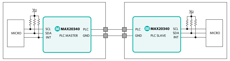
Figure 1. Simplified block diagram of the communication interface between a master and a single slave.
Transmitting Data
The MAX20340 simplifies the transmission of data over the power line. First, the data to transmit is written through I2C to the three 8-bit Transmit Data Byte registers. Then, the PLC Transmit bits are written through I2C specifying the number of bytes to transmit. The transmission starts once the PLC Transmit bits are written.
- Write up to three bytes of data to transmit into the Transmit Data Byte registers (TX_DATA0, TX_DATA1, and TX_DATA2 in registers 0x0D, 0x0E, 0x0F).
- Write the PLC Transmit bits (TX[1:0]) in the PLC_COM_CTRL register to trigger a transmit of up to three bytes. The value written to the TX[1:0] field specifies the number of bytes to transmit. (PLC_COM_CTRL in register 0x09).
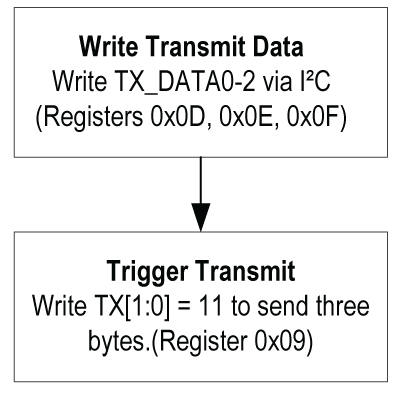
Figure 2. Flowchart showing the steps to transmit data over the power line with the MAX20340.
Receiving Data
It is also very simple to receive data sent from another MAX20340. A New Data interrupt is asserted, specifying the number of bytes received, when the data is received. The received data can then be read through I2C in the three 8-bit Receive Data Byte registers.
- Wait for the New Data interrupt (NEW_DATA1i and NEW_DATA2i in register 0x0B).
- Read up to three bytes of the received data from the Received Data Byte registers (RX_DATA0, RX_DATA1, and RX_DATA2 in registers 0x10, 0x11, and 0x12).
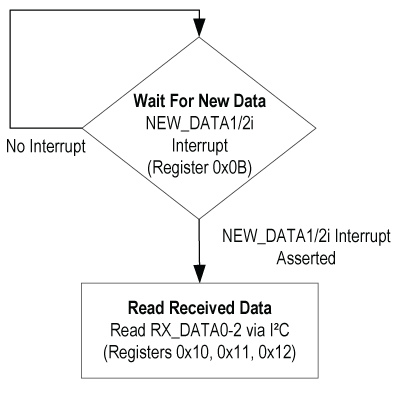
Figure 3. Flowchart showing the steps to receive the transmitted data over the power line with the MAX20340.
Master/Slave Communication Flow
In a typical application, the master and slave application processors follow the master/slave communication order and check for errors in transmission.
The MAX20340 configured as the master initiates all PLC communication. A MAX20340 configured as a slave can only transmit data to the master after the master transmits data to it. After the master transmits data, it starts a timer to wait for the slave to respond. If the timer expires, the PLC_TMRi interrupt is asserted on the master signaling the slave did not respond. The master should wait for a slave response or a timeout before sending any new data.
The master and slave should also check for transmission errors specified by the PLC_TX_ERRi and PLC_RX_ERRi interrupts.
Examples
These implementation examples assume the master and slave application processors have an input pin configured as an interrupt connected to the interrupt pin of the MAX20340. Calls to "wait_for_interrupt()" check the status of this pin and wait until it is low. Implementation of this function is platform specific. Calls to "I2C_write_register(…)" and "I2C_read_register(…)" initiate reads and writes of the 8-bit registers in the MAX20340 and their implementations are also platform specific.
It is assumed that all relevant interrupts have been unmasked in each example. Some other implementations poll interrupt registers through I2C instead of unmasking interrupts and using the interrupt pin.
These examples assume all transmissions are sent with the default communication settings: 24µs communication frequency, 288mA PLC sink current, odd parity, and 10ms RX wait timer. These settings are dependent on the application.
Transmitting Data to a Single Slave
The PLC master is connected to a single PLC slave in this example (Figure 1). The master transmits three bytes, and the slave responds with one byte. The master should only attempt to transmit data when it is in the 'Slave Found Charging' state (FSM_STAT = 0b110).
Master Transmits
The master firmware follows this basic structure to transmit three bytes after setting up the interrupt masks:
- Load a set of three bytes into the TX_DATA0-2 registers.
- Send three bytes by writing the TX[1:0] bits in the PLC_COM_CTRL register.
- Optionally, wait for the NEWDATA1/2, TMR_ERR, TX_ERR, or RX_ERR interrupt.
- Optionally, if a NEWDATA1/2 interrupt is received, read the slave response from the RX_DATA registers.
Slave Receives
After setting up the interrupt masks, the slave firmware follows this basic structure to wait for data from the master and optionally respond before the master's wait timer expires:
- Wait for the RX_ERR or NEW_DATA1/2 interrupt.
- If a NEWDATA1/2 interrupt is received, read data bytes from RX_DATA0-2 registers.
- Optionally, load the response into the TXDATA0 register.
- Optionally, send one byte by writing the TX[1:0] bits in the PLC_COM_CTRL register.
Master Transmit Firmware Sample Code Snippet
A snippet from the master firmware is shown below. The data bytes, 0x55, 0x5A, and 0xA5 are transmitted by the master in this example. This code is meant to be used as a reference to assist development and cannot be used as is.
/*Load a set of three bytes into TX_DATA0-2 registers and write all three bytes at once (I2C auto-incrementation of register address)*/
uint8_t data_bytes[3];
data_bytes[0] = 0x55;
data_bytes[1] = 0x5A;
data_bytes[2] = 0xA5;
I2C_write_register(AO23_MAST_ADDR, TX_DATA0_REG, data_bytes, 3);

/*Send three bytes by writing 0b11 to the TX[1:0] bits in the PLC_COM_CTRL register (all other bits [7:2] are application dependent)*/
I2C_write_register(AO23_MAST_ADDR, PLC_COM_CTRL_REG, 0x97);

/*Optional: wait for NEWDATA, TMR_ERR, TX_ERR, or RX_ERR interrupt (timeout should be added in typical system)*/
wait_for_interrupt();

/*Optional: Check if interrupt was caused by slave response (NEWDATA1/2)*/
uint8_t plc_int_buf[1];
I2C_read_register(AO23_MAST_ADDR, PLC_IRQ_REG, plc_int_buf, 1);
bool new_data = (plc_int_buf[0] & 0x06) != 0;

/*Optional: If NEWDATA interrupt, read single-byte slave response (response should be processed in typical system)*/
if(new_data){
    uint8_t slave_resp_buf[1];
    I2C_read_register(AO23_MAST_ADDR, RX_DATA0_REG, slave_resp_buf, 1);
}
Slave Receives Firmware Sample Code Snippet
A snippet from the slave firmware is shown below. The slave responds to the received data by transmitting a single byte: 0x55 in this example. This code is meant to be used as a reference to assist development and cannot be used as is./*Wait for RX_ERR or NEW_DATA1/2 interrupt*/
wait_for_interrupt();

/*Check if interrupt caused by received data (NEWDATA1/2)*/
uint8_t plc_int_buf[1];
I2C_read_register(AO23_SLAV_ADDR, PLC_IRQ_REG, plc_int_buf, 1);
bool new_data = (plc_int_buf[0] & 0x06) != 0;

/*If data received, read data and optionally respond*/
if(new_data){
    /*Read all three data bytes from RX_DATA0-2 registers (I2C auto-incrementation of register address) (received data should be processed in typical system)*/
    uint8_t data_reg_buf[3];
    I2C_read_register(AO23_SLAV_ADDR, RX_DATA0_REG, data_reg_buf, 3);

    /*Optional: Load response into TXDATA0 register*/
    I2C_write_register(AO23_SLAV_ADDR, TX_DATA0_REG, 0x55);

    /*Optional: Send one byte by writing the TX[1:0] bits in the PLC_COM_CTRL register (all other bits [7:2] are application dependent)*/
    I2C_write_register(AO23_SLAV_ADDR, PLC_COM_CTRL_REG, 0x95);
}
Transmitting Data to Two Slaves
The master transmits three bytes to one of the two connected slaves in this example (Figure 4).

Figure 4. Simplified block diagram of the communication interface between a master and two slaves.
Each slave is configured with different RSEL resistor values to ensure they have a unique PLC slave address. The PLC slave address of the intended recipient is added to the MSB of the first transmitted byte.
The slave responds with one byte and includes its own PLC slave address in the MSB of the response byte.
See the Multiple Slave Considerations section of this document for more details on the PLC slave addressing used in this implementation example.
Master Transmits
The master firmware follows this basic structure to transmit three bytes after setting up the master wait timer and interrupt masks:
- Load a set of three bytes into the TX_DATA0-2 registers (only 23 of the 24 bits contain the data to be sent. One bit, the MSB of TX_DATA0, contains the PLC slave address of the recipient).
- Send three bytes by writing the TX[1:0] bits in the PLC_COM_CTRL register.
- Optionally, wait for the NEWDATA1/2, TMR_ERR, TX_ERR, or RX_ERR interrupt.
- Optionally, if a NEWDATA1/2 interrupt is received, read the slave response from the RX_DATA registers.
Slave Receives
After setting up the interrupt masks, the slave firmware follows this basic structure to wait for data from the master and optionally respond before the master's wait timer expires:
- Wait for the RX_ERR or NEW_DATA1/2 interrupt.
- If a NEWDATA1/2 interrupt is received, read data bytes from the RX_DATA0-2 registers.
- Read the PS_ADD bit of the DEV_STATUS1 register.
- Check the MSB of RX_DATA0. If the MSB does not equal PS_ADD, ignore the received data.
- Optionally, load the response into the TXDATA0 register (only 7 of the 8 bits contain the data to be sent. One bit, the MSB of TX_DATA0, contains the PS_ADD bit).
- Optionally, send one byte by writing the TX[1:0] bits in the PLC_COM_CTRL register.
Master Transmit Firmware Sample Code Snippet
A snippet from the master firmware is shown below. The data bytes 0x55, 0x5A, and 0xA5 are transmitted by the master in this example. The data is transmitted to the slave with the PLC slave address '1'. So, the actual data sent is 0xD5, 0x5A, and 0xA5 (the PLC slave address is added to the MSB of Byte 1). This code is meant to be used as a reference to assist development and cannot be used as is.
/*Load a set of three bytes into TX_DATA0-2 registers and write all three bytes at once (I2C auto-incrementation of register address)*/
uint8_t data_bytes[3];
data_bytes[0] = 0xD5; /*This byte contains 7 bits of actual data, MSB is recipient PS_ADD*/
data_bytes[1] = 0x5A;
data_bytes[2] = 0xA5;
I2C_write_register(AO23_MAST_ADDR, TX_DATA0_REG, data_bytes, 3);

/*Send three bytes by writing 0b11 to the TX[1:0] bits in the PLC_COM_CTRL register (all other bits [7:2] are application dependent)*/
I2C_write_register(AO23_MAST_ADDR, PLC_COM_CTRL_REG, 0x97);

/*Optional: Wait for slave response interrupt (timeout should be added in typical system)*/
wait_for_interrupt();

/*Optional: Check if interrupt caused by slave response (NEWDATA1/2)*/
uint8_t plc_int_buf[1];
I2C_read_register(AO23_MAST_ADDR, PLC_IRQ_REG, plc_int_buf, 1);
bool new_data = (plc_int_buf[0] & 0x06) != 0;

/*Optional: if NEWDATA interrupt, read slave response (response should be processed in typical system)*/
if(new_data){
    uint8_t slave_resp_buf[1];
    I2C_read_register(AO23_MAST_ADDR, RX_DATA0_REG, slave_resp_buf, 1);
}
Slave Receives Firmware Sample Code Snippet
A snippet from the slave firmware is shown below. The slave responds to the received data by transmitting a single byte: 0x55 in this example. This slave's PLC slave address is '1'. So, the actual data sent is 0xD5 (the PLC slave address is added to the MSB of Byte 1). This code is meant to be used as a reference to assist development and cannot be used as is.
/*Wait for RX_ERR or NEW_DATA1/2 interrupt*/
wait_for_interrupt();

/*Check if interrupt caused by received data (NEWDATA1/2)*/
uint8_t plc_int_buf[1];
I2C_read_register(AO23_SLAV_ADDR, PLC_IRQ_REG, plc_int_buf, 1);
bool new_data = (plc_int_buf[0] & 0x06) != 0;

/*If data received, read data, check if intended recipient, and optionally respond*/
if(new_data){
    /*Read all three data bytes from RX_DATA0-2 registers (I2C auto-incrementation of register address) (received data should be processed in typical system)*/
    uint8_t data_reg_buf[3];
    I2C_read_register(AO23_SLAV_ADDR, RX_DATA0_REG, data_reg_buf, 3);

    /*read PS_ADD bit of the DEV_STATUS1 register*/
    uint8_t slave_addr_buf[1];
    I2C_read_register(AO23_SLAV_ADDR, DEV_STATUS1_REG, slave_addr_buf, 1);
    uint8_t PS_ADD = slave_addr_buf[0] & 0x01;

    /*Check if MSB of RX_DATA0 (intended recipient address) equals PS_ADD of this slave*/
    uint8_t = recipient_plc_addr = (data_reg_buf[0] & 0x80) >> 7;
    bool is_recipient = (PS_ADD == recipient_plc_addr);

    if(is_recipient){
        /*Optional: Load response into TXDATA0 register. This byte contains 7 bits of actual data, MSB is the slave's own PS_ADD*/
        I2C_write_register(AO23_SLAV_ADDR, TX_DATA0_REG, 0xD5);

        /*Optional: Send one byte by writing the TX[1:0] bits in the PLC_COM_CTRL register (all other bits [7:2] are application dependent)*/
        I2C_write_register(AO23_SLAV_ADDR, PLC_COM_CTRL_REG, 0x95);
    }
}
Multiple Slave Considerations
The MAX20340 master can be connected to any number of slaves. The maximum number of slaves on PLC is only limited by the maximum charge current the master can provide (1.2A) and the total capacitance on PLC.
A user-defined addressing scheme should be used to prevent multiple slaves from trying to respond at the same time when a PLC master interfaces with two or more PLC slaves. The PLC slave address is not automatically used during transmission although the RSEL resistor can be used to assign a slave with a unique PLC slave address.
When the master transmits data, all connected slaves receive the data, regardless of their configured PLC slave address. An address that uniquely identifies the intended recipient should be embedded in the data bytes when the PLC master intends to send a packet to only one of the PLC slaves. The user has the flexibility to assign the address to any bits of the data bytes.
The PLC slave address set by the RSEL is only 1-bit. So, it is only useful when addressing up to two slaves. More bits of the transmitted data bytes must be used to uniquely address all the slaves if more than two PLC slaves are connected.
All PLC slaves receive the same data. So, each slave's application processor is expected to extract the address bits from the transmitted data and compare it with its own unique address to determine if it is the intended recipient. The intended slave then processes the data accordingly while the other slaves simply discard the data.
Dual Slave Addressing Example
Assume there are two connected slaves, the first with the PLC Slave Address '0', and the second with a PLC slave address '1' (based on the RSEL value and stored in the PS_ADD bit of the DEV_STATUS1 register). The user chooses to encode the PLC slave address of the intended recipient into the most significant bit of the first byte.
The master sends 23 bits of data to the first slave as:
Byte 1: '0xxxxxxx'
Byte 2: 'xxxxxxxx'
Byte 3: 'xxxxxxxx'
where the x's are the 23 bits of data and the MSB of Byte 1 contains the PLC Slave Address ('0') of the first slave.
The master sends 23 bits of data to the second slave as:
Byte 1: '1xxxxxxx'
Byte 2: 'xxxxxxxx'
Byte 3: 'xxxxxxxx'
where the x's are the 23 bits of data and the MSB of Byte 1 contains the PLC Slave Address ('1') of the second slave.
When the master transmits this data, both slaves will receive the data.
When a slave receives the data, if the MSB of byte 1 matches the configured PLC slave address, then this data is intended for it and it should process the data. If the MSB does not match the configured PLC slave address, then this data is not intended for it and it should simply discard/ignore the data.
All other slaves also receive the response if the intended recipient slave responds to the master. The intended recipient slave's own PLC slave address should be embedded in the data bytes of the response during a slave response with multiple slaves. This ensures the other slave discards/ignores the intended slave's response to the master.
Note that this is not required and there is no slave addressing built into the PLC protocol. If the user application does not require the two slaves to receive different data and slaves never try to respond to the master at the same time, the unique address does not need to be embedded in the data bytes. Both slaves receive the data sent by the master if no slave addressing scheme is used. If any slave responds to the master, all other slaves see this response as received data. Communication errors occur if two slaves try to respond at the same time. A proper slave addressing scheme prevents errors like this.