Bluetooth Power Amplifier: System Performance Review
Abstract
The MAX2240 power amplifier (PA) is characterized for Bluetooth® operation. Performance is presented for the following areas: Transmit output spectrum, 1dB compression point, S-parameters, noise figure, harmonic output content, gain and supply current. Bluetooth uses GFSK modulation between 2.402GHz and 2.48GHz. The PA output power is +20dBm and includes output power control circuitry.
Introduction
Bluetooth communication is a TDD (time-division duplex) system that operates in the ISM band, between 2.402GHz and 2.48GHz. The Bluetooth system uses a digital-frequency-modulation method known as 0.5BT GFSK (Gaussian frequency-shift keying). With this type of modulation, the carrier is shifted up by 175kHz to represent a "1" and down by 175kHz to represent a "0", typically at a rate of 1M symbols per second. The 0.5BT (bandwidth time) defines the 3dB bandwidth at half the data rate, which is 500kHz. The system adapts FHSS (frequency-hopping spread spectrum) to improve the RF link's quality and reliability. The hopping rate is up to 1600hops/sec. In GFSK modulation, the signal is contained in the constant amplitude envelope; thus, the PA (power amplifier) is allowed to drive into saturation to deliver transmit power with high efficiency.
Analog Devices' MAX2240 single-supply, low-voltage, power-amplifier IC is ideal for Bluetooth application. This PA provides a nominal +20dBm (100mW) output power. Additionally, the PA includes a digital-power-control circuit. There are four digitally controlled output-power levels, making the PA compliant with Bluetooth Class-1 and Class-2 power. A digital input controls the active and shutdown operating modes to efficiently operate the PA in the TDD system. The MAX2240 integrates the RF input and interstage matching, simplifying the application of the IC and minimizing the area of the PCB (printed-circuit board).
Required PA Characterization for Bluetooth
Transmit Output Spectrum: Measurements for the transmit output spectrum analyze the power levels in the frequency domain to ensure that, under given conditions, the PA will meet the FCC 20dB bandwidth requirements (FCC 15.247) and the Bluetooth transmit spectrum-mask requirements (see Table 1 for details).
- Transmit Output Spectrum vs. VCC (see Test-Results A, B, C, and D)
- Transmit Output Spectrum vs. Gain Control Level (see Test-Results A, B, C, and D)
- Transmit Output Spectrum vs. Input Power Ramping (see Test-Result E): Due to the typical AM-PM (amplitude modulation-phase modulation) nonlinearly effect of the PA, input-power-ramping speed determines the transient output-power spectrum. When the ramping speed is over the limit, the AM-PM nonlinearly effect will cause a growth in the spectral output. This new spectral growth must be controlled so as to stay below the in-band spurious-emission requirements specified by Bluetooth.
1dB Compression-Point Measurements (see Test-Result F)
Small-Signal S-Parameter Measurements (see Test-Result G): Because the MAX2240 is a typical Class-A PA, the device characteristic will be different depending on the input to the PA. The measurements are taken using an HP 8753E network analyzer. Therefore, the S22 does not represent the actual output matching due to the transient behavior of the network analyzer. The 20dB load/pad is compensated for by calibration of the network analyzer to include its effect.
Noise Figure of the PA (see Test-Result H): Characterizes the total thermal-noise power due to the PA.
Noise-Power Measurements (see Test-Result I): Characterizes the noise power emission over a wide frequency range.
Harmonic Measurements (see Test-Result J)
PIN vs. POUT Measurements and PIN vs. ICC Measurements (see Test-Result K)
| Frequency Offset | Transmit Power |
| ±550kHz | -20dBc |
| | M - N | = 2 | -20dBm |
| | M - N | > = 3 | -40dBm |
MAX2240 PA Performance Review
Overall Test Conditions:
- All tests are performed at room temperature.
- Type of modulation: Bluetooth, GFSK with 0.5BT and 175kHz frequency deviation.
- For detailed product information, refer to the MAX2240 data sheet.
Bench-Setup Block Diagrams

Figure 1. Bench setup for output power, output spectrum, and harmonic and P1db measurements.

Figure 2. Bench setup for spectral splattering measurements.

Figure 3. Bench setup for small-signal S-parameter measurements.

Figure 4. Bench setup for noise-figure measurements.
Test Results
Test-Result A
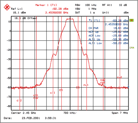
Figure 5. Maximum output at 2.45GHz with 4dBm input power, with VCC = 3.2V.
Test-Result B
| Frequency | PIN | DO | D1 | ICC | POUT | ±550kHz | ±1.5MHz | ±2.5MHz |
| GHz | dBm | mA | dBm | dBc | dBm | dBm | ||
| 2.42 | -2 | 0 | 0 | 66.97 | -4.56 | -22.34 | -48.00 | -52.87 |
| 0 | 1 | 73.59 | 9.54 | -22.67 | -35.72 | -52.27 | ||
| 1 | 0 | 68.88 | 2.75 | -21.00 | -42.14 | -52.64 | ||
| 1 | 1 | 94.70 | 17.14 | -22.34 | -28.29 | -50.91 | ||
| 0 | 0 | 0 | 68.28 | -1.12 | -23.17 | -23.33 | -52.73 | |
| 0 | 1 | 75.36 | 10.78 | -23.16 | -34.46 | -52.04 | ||
| 1 | 0 | 70.19 | 4.96 | -21.66 | -40.18 | -52.50 | ||
| 1 | 1 | 100.40 | 18.13 | -23.33 | -27.16 | -50.67 | ||
| 2 | 0 | 0 | 69.90 | 2.14 | -23.66 | -42.68 | -52.78 | |
| 0 | 1 | 78.07 | 12.10 | -24.50 | -33.31 | -51.86 | ||
| 1 | 0 | 71.99 | 7.19 | -24.17 | -38.09 | -52.43 | ||
| 1 | 1 | 106.33 | 18.99 | -21.50 | -26.21 | -50.39 | ||
| 2.45 | -2 | 0 | 0 | 66.82 | -4.77 | -22.66 | -48.18 | -53.03 |
| 0 | 1 | 73.34 | 9.45 | -21.34 | -35.80 | -52.30 | ||
| 1 | 0 | 68.70 | 2.55 | -23.33 | -42.42 | -52.77 | ||
| 1 | 1 | 93.33 | 17.04 | -22.67 | -28.36 | -50.88 | ||
| 0 | 0 | 0 | 68.01 | -1.47 | -21.67 | -45.64 | -52.88 | |
| 0 | 1 | 74.98 | 10.64 | -24.67 | -34.69 | -52.18 | ||
| 1 | 0 | 69.96 | 4.73 | -22.50 | -40.41 | -52.66 | ||
| 1 | 1 | 99.08 | 17.89 | -20.17 | -27.55 | -50.82 | ||
| 2 | 0 | 0 | 69.61 | 1.61 | -20.50 | -43.17 | -52.68 | |
| 0 | 1 | 77.49 | 11.85 | -23.66 | -33.55 | -52.03 | ||
| 1 | 0 | 71.67 | 6.84 | -20.83 | -38.42 | -52.60 | ||
| 1 | 1 | 104.88 | 18.90 | -22.16 | -26.51 | -50.45 | ||
| 2.48 | -2 | 0 | 0 | 66.88 | -4.47 | -22.67 | -48.11 | -53.12 |
| 0 | 1 | 73.31 | 9.57 | -22.67 | -35.74 | -52.41 | ||
| 1 | 0 | 68.78 | 2.69 | -22.00 | -42.32 | -52.83 | ||
| 1 | 1 | 92.61 | 17.01 | -22.16 | -28.36 | -50.96 | ||
| 0 | 0 | 0 | 68.12 | -1.32 | -19.67 | -45.70 | -53.01 | |
| 0 | 1 | 74.97 | 10.68 | -22.34 | -34.81 | -52.20 | ||
| 1 | 0 | 70.04 | 4.93 | -20.67 | -40.64 | -52.78 | ||
| 1 | 1 | 98.30 | 18.09 | -22.67 | -27.31 | -50.74 | ||
| 2 | 0 | 0 | 69.73 | 2.06 | -24.16 | -42.88 | -52.95 | |
| 0 | 1 | 77.49 | 12.07 | -20.50 | -33.28 | -51.98 | ||
| 1 | 0 | 71.78 | 6.96 | -23.00 | -38.41 | -52.56 | ||
| 1 | 1 | 104.12 | 18.96 | -23.17 | -26.46 | -50.64 |
Test-Result C
| Frequency | PIN | DO | D1 | ICC | POUT | ±550kHz | ±1.5MHz | ±2.5MHz |
| GHz | dBm | mA | dBm | dBc | dBm | dBm | ||
| 2.42 | -2 | 0 | 0 | 64.23 | -4.80 | -22.50 | -47.78 | -52.68 |
| 0 | 1 | 71.24 | 9.41 | -21.84 | -35.27 | -52.07 | ||
| 1 | 0 | 66.20 | 2.56 | -24.83 | -41.79 | -52.64 | ||
| 1 | 1 | 94.74 | 17.24 | -22.33 | -27.56 | -50.74 | ||
| 0 | 0 | 0 | 65.53 | -1.39 | -22.00 | -45.53 | -52.73 | |
| 0 | 1 | 73.21 | 10.51 | -24.00 | -34.75 | -52.03 | ||
| 1 | 0 | 67.58 | 4.68 | -23.67 | -40.40 | -52.52 | ||
| 1 | 1 | 99.99 | 18.09 | -24.83 | -27.07 | -50.62 | ||
| 2 | 0 | 0 | 67.12 | 1.89 | -22.16 | -42.83 | -52.73 | |
| 0 | 1 | 76.00 | 11.89 | -22.17 | -33.32 | -51.84 | ||
| 1 | 0 | 69.34 | 6.86 | -20.67 | -38.06 | -52.44 | ||
| 1 | 1 | 104.86 | 18.74 | -22.83 | -26.41 | -50.37 | ||
| 2.45 | -2 | 0 | 0 | 64.00 | -5.03 | -20.66 | -48.36 | -52.98 |
| 0 | 1 | 70.87 | 9.24 | -21.50 | -36.10 | -52.31 | ||
| 1 | 0 | 65.92 | 2.36 | -22.50 | -42.50 | -52.79 | ||
| 1 | 1 | 92.98 | 17.04 | -21.34 | -28.29 | -50.98 | ||
| 0 | 0 | 0 | 65.26 | -1.67 | -22.34 | -45.90 | -52.90 | |
| 0 | 1 | 72.72 | 10.32 | -22.00 | -34.95 | -52.20 | ||
| 1 | 0 | 67.27 | 4.47 | -20.67 | -40.55 | -52.53 | ||
| 1 | 1 | 98.49 | 17.86 | -22.84 | -27.52 | -50.74 | ||
| 2 | 0 | 0 | 66.34 | 1.61 | -21.16 | -43.16 | -52.76 | |
| 0 | 1 | 75.41 | 11.65 | -21.84 | -33.51 | -51.96 | ||
| 1 | 0 | 69.05 | 6.62 | -21.67 | -38.62 | -52.38 | ||
| 1 | 1 | 103.36 | 18.68 | -20.00 | -26.54 | -50.41 | ||
| 2.48 | -2 | 0 | 0 | 64.05 | -4.94 | -23.33 | -48.33 | -53.12 |
| 0 | 1 | 70.85 | 9.29 | -21.83 | -36.07 | -52.34 | ||
| 1 | 0 | 65.98 | 2.45 | -23.00 | -42.49 | -52.85 | ||
| 1 | 1 | 92.24 | 16.94 | -22.16 | -47.89 | -53.16 | ||
| 0 | 0 | 0 | 65.29 | -1.49 | -24.33 | -45.80 | -53.12 | |
| 0 | 1 | 72.68 | 10.51 | -23.66 | -34.84 | -52.22 | ||
| 1 | 0 | 67.34 | 4.62 | -23.16 | -40.52 | -52.73 | ||
| 1 | 1 | 97.52 | 17.91 | -20.50 | -27.35 | -50.77 | ||
| 2 | 0 | 0 | 66.92 | 1.88 | -22.00 | -43.00 | -52.92 | |
| 0 | 1 | 75.37 | 11.75 | -18.00 | -33.71 | -52.19 | ||
| 1 | 0 | 69.13 | 6.77 | -23.34 | -38.60 | -52.56 | ||
| 1 | 1 | 102.10 | 18.62 | -19.50 | -26.75 | -50.63 |
Test-Result D
| Frequency | PIN | DO | D1 | ICC | POUT | ±550kHz | ±1.5MHz | ±2.5MHz |
| GHz | dBm | mA | dBm | dBc | dBm | dBm | ||
| 2.42 | -2 | 0 | 0 | 60.98 | -4.95 | -22.17 | -47.88 | -52.88 |
| 0 | 1 | 68.17 | -8.94 | -20.16 | -35.76 | -52.12 | ||
| 1 | 0 | 62.83 | -2.06 | -23.67 | -42.30 | -52.64 | ||
| 1 | 1 | 90.53 | -16.69 | -23.67 | -28.16 | -50.73 | ||
| 0 | 0 | 0 | 62.28 | -1.54 | -22.00 | -45.23 | -52.70 | |
| 0 | 1 | 70.21 | 10.20 | -23.50 | -34.57 | -51.98 | ||
| 1 | 0 | 64.36 | 4.24 | -20.67 | -40.08 | -52.42 | ||
| 1 | 1 | 93.82 | 17.24 | -22.67 | -27.63 | -50.69 | ||
| 2 | 0 | 0 | 63.86 | 1.86 | -25.50 | -43.13 | -54.21 | |
| 0 | 1 | 73.66 | 11.66 | -23.34 | -33.23 | -51.75 | ||
| 1 | 0 | 66.30 | 6.62 | -23.50 | -38.35 | -53.64 | ||
| 1 | 1 | 96.25 | 17.47 | -24.50 | -27.31 | -50.70 | ||
| 2.45 | -2 | 0 | 0 | 60.75 | -5.61 | -22.50 | -48.27 | -52.99 |
| 0 | 1 | 68.14 | 9.02 | -26.00 | -35.74 | -52.30 | ||
| 1 | 0 | 62.74 | 1.71 | -21.33 | -42.61 | -52.80 | ||
| 1 | 1 | 89.21 | 16.54 | -25.00 | -28.40 | -51.12 | ||
| 0 | 0 | 0 | 61.95 | -2.29 | -24.84 | -46.12 | -52.99 | |
| 0 | 1 | 69.95 | 1.19 | -22.50 | -34.65 | -52.07 | ||
| 1 | 0 | 64.20 | 4.26 | -18.33 | -40.51 | -52.69 | ||
| 1 | 1 | 91.79 | 17.08 | -26.33 | -27.80 | -50.81 | ||
| 2 | 0 | 0 | 63.71 | 1.46 | -25.33 | -42.88 | -52.80 | |
| 0 | 1 | 72.66 | 11.39 | -21.33 | -33.51 | -52.02 | ||
| 1 | 0 | 65.80 | 6.16 | -25.50 | -38.45 | -52.45 | ||
| 1 | 1 | 94.64 | 17.31 | -24.50 | -27.55 | -51.03 | ||
| 2.48 | -2 | 0 | 0 | 60.73 | -5.49 | -22.83 | -47.97 | -52.99 |
| 0 | 1 | 68.14 | 9.08 | -20.16 | -35.80 | -52.40 | ||
| 1 | 0 | 62.89 | 2.24 | -20.00 | -42.14 | -52.83 | ||
| 1 | 1 | 88.67 | 16.60 | -24.34 | -27.95 | -51.06 | ||
| 0 | 0 | 0 | 62.18 | -1.62 | -21.83 | -45.45 | -53.00 | |
| 0 | 1 | 70.05 | 10.27 | -24.16 | -34.56 | -52.18 | ||
| 1 | 0 | 64.29 | 4.44 | -21.83 | -40.19 | -52.70 | ||
| 1 | 1 | 91.25 | 17.05 | -23.00 | -27.81 | -51.16 | ||
| 2 | 0 | 0 | 63.92 | 1.72 | -20.33 | -42.75 | -52.86 | |
| 0 | 1 | 72.93 | 11.55 | -22.00 | -33.32 | -52.13 | ||
| 1 | 0 | 66.22 | 6.65 | -18.33 | -37.94 | -52.53 | ||
| 1 | 1 | 93.68 | 17.30 | -24.33 | -27.54 | -50.99 |
Test-Result E: Spectral Splattering Measurements

Figure 6. Output spectrum with 10µs ramping time.

Figure 7. Output spectrum with 5µs ramping time.

Figure 8. Output spectrum with 1µs ramping time.

Figure 9. Time-domain output spectrum with -1.5MHz offset (worst case).

Figure 10. Time-domain output spectrum with -2.5MHz offset (worst case).
Test-Result F: P1dB Measurements
| VCC = 2.7V | VCC = 3.6V | ||||||
| D0, D1 = 1, 1 | D0, D1 = 1, 1 | ||||||
| PIN | PIN, Cal | POUT | Gain | PIN | PIN, Cal | POUT | Gain |
| dBm | dBm | dBm | dB | dBm | dBm | dBm | dB |
| -9.58 | -11 | 9.85 | 20.85 | -9.58 | -11 | 10 | 21 |
| -8.58 | -10 | 10.76 | 20.76 | -8.58 | -10 | 10.94 | 20.94 |
| -7.58 | -9 | 11.63 | 20.63 | -7.58 | -9 | 11.82 | 20.82 |
| -6.58 | -8 | 12.48 | 20.48 | -6.58 | -8 | 12.68 | 20.68 |
| -5.58 | -7 | 13.33 | 20.33 | -5.58 | -7 | 13.51 | 20.51 |
| -4.58 | -6 | 14.12 | 20.12 | -4.58 | -6 | 14.34 | 20.34 |
| -3.58 | -5 | 14.87 | 19.87 | -3.58 | -5 | 15.09 | 20.09 |
| -2.58 | -4 | 15.57 | 19.57 | -2.58 | -4 | 15.85 | 19.85 |
| -1.58 | -3 | 16.09 | 19.09 | -1.58 | -3 | 16.52 | 19.52 |
| -0.58 | -2 | 16.55 | 18.55 | -0.58 | -2 | 17.13 | 19.13 |
| 0.42 | -1 | 16.83 | 17.83 | 0.42 | -1 | 17.67 | 18.67 |
| 1.42 | 0 | 17 | 17 | 1.42 | 0 | 18.14 | 18.14 |
| 2.42 | 1 | 17.16 | 16.16 | 2.42 | 1 | 18.59 | 17.59 |
| 3.42 | 2 | 17.34 | 15.34 | 3.42 | 2 | 19.01 | 17.01 |
| 4.42 | 3 | 17.42 | 14.42 | 4.42 | 3 | 19.32 | 16.32 |
| 5.42 | 4 | 17.5 | 13.5 | 5.42 | 4 | 19.72 | 15.72 |
| 6.42 | 5 | 17.67 | 12.67 | 6.42 | 5 | 20.04 | 15.04 |
| 7.42 | 6 | 17.74 | 11.74 | 7.42 | 6 | 20.3 | 14.3 |
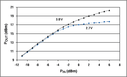
Figure 11. PIN vs. POUT.
Test-Result G: Small-Signal S-Parameters
| 2.42GHz | 2.45GHz | 2.48GHz | ||||
| VCC = 3.6V | VCC = 2.7V | VCC = 3.6V | VCC = 2.7V | VCC = 3.6V | VCC = 2.7V | |
| 20 log |S11| | -16.6dB | -14.1dB | -16.9dB | -14.2dB | -18.6dB | -14.3dB |
| 20 log |S21| | 18.6dB | 17.3dB | 18.6dB | 17.2dB | 18.5dB | 17.0dB |
| 20 log |S12| | -50.3dB | -48.2dB | -48.9dB | -47.7dB | -47.6dB | -45.3dB |
| 20 log |S22| | -2.9dB | -3.0dB | -2.7dB | -2.9dB | -2.8dB | -3.2dB |
Test-Result H: Noise-Figure Measurements
| Frequency | D0 | D1 | NF (dB) | |
| GHz | VCC = 3.6V | VCC = 2.7V | ||
| 2.42 | 0 | 0 | -- | -- |
| 1 | 0 | 13.3 | 13.4 | |
| 0 | 1 | 9.3 | 9.2 | |
| 1 | 1 | 5.8 | 5.7 | |
| 2.45 | 0 | 0 | -- | -- |
| 1 | 0 | 13.5 | 13.5 | |
| 0 | 1 | 9.4 | 9.3 | |
| 1 | 1 | 5.9 | 5.8 | |
| 2.48 | 0 | 0 | -- | -- |
| 1 | 0 | 13.5 | 13.6 | |
| 0 | 1 | 9.5 | 9.4 | |
| 1 | 1 | 6.0 | 5.9 | |
Test-Result I: Noise-Power Measurements
Test Conditions:
- VCC = 3.2V
- FIN = 2.45GHz
- PIN = +4dBm
- POUT = +19.53dBm

Figure 12. Noise-power-measurement graph.
Test-Result J: Harmonic Measurements
Test Conditions:
- VCC = 3.2V
- FIN = 2.45GHz
- PIN = +4dBm
- POUT = +19.53dBm
| Harmonic Freq (GHz) | Power (dBm, RBW = 100kHz measured on Agilent [HP] 8562EC) | Power (dBm, 1MHz CH BW measured on R&S FSEA, limited at 6GHz) |
| 4.80 | -28.16 | -25.74 |
| 7.20 | -15.00 | N/A |
| 9.60 | -37.16 | N/A |
| 12.00 | -42.00 | N/A |
Test-Result K: POUT vs. PIN Measurements (at Maximum Gain with 3.2-Volt VCC)

Figure 13. PIN vs. POUT and PIN vs. ICC, Board #1.
The MAX2240 Evaluation Board: Schematic and Layout
 For larger image
Figure 14. Schematic.

Figure 15. Top-level only layout. For detailed layout information, refer to the MAX2240 data sheet
CSP (Chip-Scale Package) Recommended PCB Design
Pad size: 10-mil diameter
Pitch: 19.7 mils
Trace width for middle-pin routing: 3 mils
Solder-mask opening: 14-mil diameter for precise alignment, 16-mil diameter
in general

Figure 16. Pitch and pad size.
Refer to the application note 1891, "Wafer-Level Packaging (WLP) and Its Applications."