AN-2064: ADF7030-1 Receiver Desense Avoidance Algorithm
INTRODUCTION
Integrated system on chip (SoC) transceivers always exhibit spurious phenomena due to finite isolation between clock sources and sensitive analog and RF circuitry. These spurious phenomena may cause degraded sensitivity (desense) when the transceiver is operating in receive mode on specific channels. The traditional approach to addressing desense is to avoid these degraded channels by blacklisting them from the channel plan. However, reducing the number of channels may reduce the network capacity and, in frequency hopping applications, the ability of the network to avoid interference.
This application note describes a simple software algorithm for the ADF7030-1 that robustly mitigates against desense caused by certain spurious phenomena. This software algorithm avoids the need to blacklist channels and therefore allows more usage of the allowed spectrum.
ADF7030-1
If the ADF7030-1 receiver must operate in a channelized system over wide frequency bands such as 902 MHz to 928 MHz, 863 MHz to 876 MHz, or 450 MHz to 470 MHz, a small number of specific frequencies exhibit desense due to spurious phenomena.
In general, the cause of the sensitivity degradation is attributed to the following spurious phenomena:
- A raw harmonic of a clock source falls within the bandwidth of the receiver.
- A harmonic of an internal clock mixes with a higher order harmonic of the local oscillator (LO) and falls within the bandwidth of the receiver at baseband.
The software algorithm requires the host to modify certain receiver settings before using one of the channel frequencies exhibiting an issue with desense. The modified receiver settings make use of several on-chip features to move the source of the interference outside the bandwidth of the receiver, thereby allowing the ADF7030-1 receiver to reach the full sensitivity potential on that channel.
REGISTER SETTINGS
The PROFILE_RADIO_DIG_RX_CFG and PROFILE_RADIO_AFC_CFG2 registers contain the receiver settings that must be modified as part of the software algorithm that runs on the host processor. Table 1 and Table 2 describe the bit fields in each of these registers. The software algorithm uses these bit fields.
RECEIVER CONFIGURATION REGISTER
Address: 0x20000300, Reset: 0x00000000, Name: PROFILE_RADIO_DIG_RX_CFG
| Bits | Bit Name | Description | Reset | Access |
| [31:30] | DEMOD_SCALING | Generated by the ADF7030-1 design center or provided by Analog Devices, Inc. | 0x0 | R/W |
| [29:27] | Reserved | Set to 0. | 0x0 | R/W |
| 26 | Invert | 0: configure demodulation with dot product. 1: configure demodulation with cross product. |
0x0 | R/W |
| [25:22] | ADC_ANALOG_CLK_DIVIDE | Divide down ratio of Σ-Δ analog-to-digital converter (ADC) clock relative to the master clock rate. | 0x0 | R/W |
| [21:18] | DECIMATE_8XIF_CLK_DIVIDE | Divide down ratio of DECIMATE_8XIF_CLK relative to the master clock. | 0x0 | R/W |
| 17 | LOW_SIDE | Select high sided or low sided injection. 0: high sided injection. 1: low sided injection. |
0x0 | R/W |
| [16:13] | DEMOD_CORE_CLK_DIVIDE | Divide down ratio of the demodulation core clock relative to the master clock. | 0x0 | R/W |
| 12 | DEMOD_PRODUCT_SEL | Dot/cross product select. | 0x0 | R/W |
| [11:8] | DEMOD_POST_DEMOD_FILTER_BW | Generated by the ADF7030-1 design center or provided by Analog Devices. | 0x0 | R/W |
| [7:0] | DEMOD_DISC_BW | Receiver discriminator bandwidth. | 0x0 | R/W |
AUTOMATIC FREQUENCY CONTROL (AFC) CONFIGURATION REGISTER 2
Address: 0x20000320, Reset: 0x00000003, Name: PROFILE_RADIO_AFC_CFG2
| Bits | Bit Name | Description | Reset | Access |
| [31:30] | Reserved | Reserved. | 0x0 | R |
| 29 | AFC_PRODUCT_SEL | Generated by the ADF7030-1 design center or provided by Analog Devices. | 0x0 | R/W |
| 28 | AFC_INVERT | AFC invert. | 0x0 | R/W |
| [27:22] | AFC_BW | AFC measurement bandwidth (BW). | 0x0 | R/W |
| [21:19] | AFC_SAMPLE_RATE | Generated by the ADF7030-1 design center or provided by Analog Devices. | 0x0 | R/W |
| [18:3] | AFC_INITIAL_CONDITION | Generated by the ADF7030-1 design center or provided by Analog Devices. | 0x0 | R/W |
| [2:0] | AFC_MODE | Generated by the ADF7030-1 design center or provided by Analog Devices. | 0x3 | R/W |
DESENSE FREQUENCIES ACROSS THE FCC PART 15 BAND—902 MHz TO 928 MHz
USE CASES
Table 3 describes the seven use cases that are explored in this application note. The receiver and desense bandwidths are also included. The desense bandwidth is set to be 1.5 times the receiver bandwidth.
| Use Case | Data Rate (kbps) | Frequency Deviation (kHz) | Maximum Frequency Error (ppm) | Intermediate Frequency (kHz) | Receiver Bandwidth (kHz) | Desense Bandwidth (kHz) |
| UC10 | 10 | 5.0 | 10 | 81.25 | 20.0 | 30.0 |
| UC12p5 | 12.5 | 50.0 | 10 | 180.55 | 135.42 | 203.13 |
| UC25 | 25 | 6.3 | 10 | 103.17 | 77.38 | 116.07 |
| UC50 | 50 | 25.0 | 10 | 135.42 | 101.57 | 152.35 |
| UC100 | 100 | 25.0 | 13 | 180.55 | 135.42 | 203.13 |
| UC150 | 150 | 37.5 | 25 | 270.83 | 203.12 | 304.68 |
| UC300 | 300 | 75.0 | 10 | 406.25 | 395.00 | 592.50 |
CLASSIFICATION
Table 4 to Table 10 describe the channel frequencies for the seven use cases in the 902 MHz to 928 MHz band that typically exhibit receiver desense due to spurious phenomena. Each frequency is classified, and this classification is used in the software algorithm.
| Frequency (MHz) | Cause of Receiver Sensitivity Degradation | Software Algorithm Able to Address Problem | Classification for Software Algorithm |
| 903.5 | ADC clock harmonic | Yes | ADC_DESENSE_CHAN |
| 910.0 | Harmonic of 26 MHz crystal (XTAL) | No | Not applicable |
| 916.5 | ADC clock harmonic | Yes | ADC_DESENSE_CHAN |
| 923.0 | ADC clock harmonic | Yes | ADC_DESENSE_CHAN |
| Frequency (MHz) | Cause of Receiver Sensitivity Degradation | Software Algorithm Able to Address Problem | Classification for Software Algorithm |
| 903.5 | ADC clock harmonic | Yes | ADC_DESENSE_CHAN |
| 905.9 | Mixing of clock and LO harmonics | Yes | CLOCK_LO_HARM_DESENSE_CHAN |
| 910.0 | Harmonic of 26 MHz XTAL | No | Not applicable |
| 912.4 | Mixing of clock and LO harmonics | Yes | CLOCK_LO_HARM_DESENSE_CHAN |
| 916.5 | ADC clock harmonic | Yes | ADC_DESENSE_CHAN |
| 918.9 | Mixing of clock and LO harmonics | Yes | CLOCK_LO_HARM_DESENSE_CHAN |
| 923.0 | ADC clock harmonic and demodulator clock harmonic | Yes | ADC_DESENSE_CHAN and DEMOD_DESENSE_CHAN |
| Frequency (MHz) | Cause of Receiver Sensitivity Degradation | Software Algorithm Able to Address Problem | Classification for Software Algorithm |
| 903.5 | ADC clock harmonic | Yes | ADC_DESENSE_CHAN |
| 905.8 | Mixing of clock and LO harmonics | Yes | CLOCK_LO_HARM_DESENSE_CHAN |
| 910.0 | Harmonic of 26 MHz XTAL | No | Not applicable |
| 912.3 | Mixing of clock and LO harmonics | Yes | CLOCK_LO_HARM_DESENSE_CHAN |
| 916.5 | ADC clock harmonic | Yes | ADC_DESENSE_CHAN |
| 918.8 | Mixing of clock and LO harmonics | Yes | CLOCK_LO_HARM_DESENSE_CHAN |
| 923.0 | ADC clock harmonic and demodulator clock harmonic | Yes | ADC_DESENSE_CHAN and DEMOD_DESENSE_CHAN |
| 925.3 | Mixing of clock and LO harmonics | Yes | CLOCK_LO_HARM_DESENSE_CHAN |
| Frequency (MHz) | Cause of Receiver Sensitivity Degradation | Software Algorithm Able to Address Problem | Classification for Software Algorithm |
| 903.5 | ADC clock harmonic | Yes | ADC_DESENSE_CHAN |
| 910.0 | Harmonic of 26 MHz XTAL | No | Not applicable |
| 914.5 | Mixing of clock and LO harmonics | Yes | CLOCK_LO_HARM_DESENSE_CHAN |
| 916.5 | ADC clock harmonic | Yes | ADC_DESENSE_CHAN |
| 923.0 | ADC clock harmonic and demodulator clock harmonic | Yes | ADC_DESENSE_CHAN and DEMOD_DESENSE_CHAN |
| 927.5 | Mixing of clock and LO harmonics | Yes | CLOCK_LO_HARM_DESENSE_CHAN |
| Frequency (MHz) | Cause of Receiver Sensitivity Degradation | Software Algorithm Able to Address Problem | Classification for Software Algorithm |
| 903.5 | ADC clock harmonic | Yes | ADC_DESENSE_CHAN |
| 905.9 | Mixing of clock and LO harmonics | Yes | CLOCK_LO_HARM_DESENSE_CHAN |
| 910.0 | Harmonic of 26 MHz XTAL | No | Not applicable |
| 916.5 | ADC clock harmonic | Yes | ADC_DESENSE_CHAN |
| 918.9 | Mixing of clock and LO harmonics | Yes | CLOCK_LO_HARM_DESENSE_CHAN |
| 923.0 | ADC clock harmonic and demodulator clock harmonic | Yes | ADC_DESENSE_CHAN and DEMOD_DESENSE_CHAN |
| 927.6 | Mixing of clock and LO harmonics | Yes | CLOCK_LO_HARM_DESENSE_CHAN |
| Frequency (MHz) | Cause of Receiver Sensitivity Degradation | Software Algorithm Able to Address Problem | Classification for Software Algorithm |
| 903.5 | ADC clock harmonic | Yes | ADC_DESENSE_CHAN |
| 906.0 | Mixing of clock and LO harmonics | Yes | CLOCK_LO_HARM_DESENSE_CHAN |
| 910.0 | Harmonic of 26 MHz XTAL | No | Not applicable |
| 916.5 | ADC clock harmonic | Yes | ADC_DESENSE_CHAN |
| 923.0 | ADC clock harmonic and demodulator clock harmonic | Yes | ADC_DESENSE_CHAN and DEMOD_DESENSE_CHAN |
| 927.7 | Mixing of clock and LO harmonics | Yes | CLOCK_LO_HARM_DESENSE_CHAN |
| Frequency (MHz) | Cause of Receiver Sensitivity Degradation | Software Algorithm Able to Address Problem | Classification for Software Algorithm |
| 903.5 | ADC clock harmonic | Yes | ADC_DESENSE_CHAN |
| 903.7 | Mixing of clock and LO harmonics | Yes | CLOCK_LO_HARM_DESENSE_CHAN |
| 910.0 | Harmonic of 26 MHz XTAL | No | Not applicable |
| 910.5 | Mixing of clock and LO harmonics | Yes | CLOCK_LO_HARM_DESENSE_CHAN |
| 916.5 | ADC clock harmonic | Yes | ADC_DESENSE_CHAN |
| 923.0 | ADC clock harmonic and demodulator clock harmonic | Yes | ADC_DESENSE_CHAN and DEMOD_DESENSE_CHAN |
| 923.5 | Mixing of clock and LO harmonics | Yes | CLOCK_LO_HARM_DESENSE_CHAN |
| 927.9 | Mixing of clock and LO harmonics | Yes | CLOCK_LO_HARM_DESENSE_CHAN |
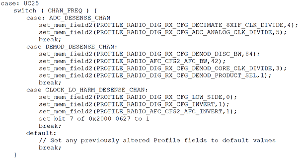
HOST SOFTWARE ALGORITHM
With reference to Table 4 to Table 10, the following pseudo C code conceptually illustrates how a host can alter the ADF7030-1 radio profile based on the desired channel frequency for desense avoidance. Make these radio profile setting modifications in PHY_ON prior to issuing the CMD_PHY_RX command. There is no requirement to issue the CMD_CFG_DEV after modifying these settings.


RESULTS FOR COMBINED TRANSMITTER/RECEIVER MATCH
The evaluation board used for this testing has a suboptimal RF match. Therefore, the baseline receive sensitivity is not representative of the best achievable performance.


Authors

