AN-2020: An EMC Robust PCB Design Based on the AD7606B ADC for Power Automated Applications
Introduction
The AD7606B is a 16-bit, simultaneous sampling, analog-to-digital data acquisition system (DAS) with eight channels. Each channel contains a successive approximation register (SAR), analog-todigital converter (ADC). The AD7606B is designed to be used in power automation systems such as protection relay systems, merging unit systems, and other secondary power automation devices in harsh environments. For these systems, electromagnetic compatibility (EMC) design is a top priority.
This application note provides an EMC board level design and a guide for using the AD7606B as a standard analog front end (AFE) for interfacing the current and voltage sensing circuits.
Typical Use Case of the AD7606B in a Power Automated System
Figure 1 shows a typical use case of the AD7606B in a power automated system. In the standard configuration, the AD7606B connects to the current or voltage transformers via a simple RCbased low-pass filter.
In some low voltage applications, such as a 220 V to 380 V ac power metering system, the resistor divider network can replace the voltage transformers for voltage measurement (see Figure 2). The AFE components must be robust enough to survive an electrical impact from the power grid because the circuit input is connected directly to the power grid without isolation.


EMC Standards
Typically, there are several types of electrical impacts present on power mains. To test the robustness of the AD7606B, three EMC standard electrical impacts are applied to the AD7606B-based EMC test board.
IEC 61000-4-2: Electrostatic Discharge (ESD)
One of the electrical impacts tested on the AD7606B-based EMC test board is the IEC 61000-4-2 electrostatic discharge (ESD) standard. ESD surges affect most power automated equipment. The ESD testing simulates the sudden flow of electricity between two electrically charged objects caused by contact, an electrical short, or a dielectric breakdown.
The IEC 61000-4-2 standard is tested through the contact discharge and air discharge methods. The contact discharge method is tested at four standard levels ranging from 2 kV to 8 kV. The air discharge method is tested from 2 kV to 15 kV. The power automation equipment must pass a Level 4 ESD impact, so an 8 kV contact discharge and a 15 kV air discharge are applied to the AD7606B testing board to verify the robustness of the device. For details regarding the ESD testing setup and the ESD testing waveform, refer to the IEC 61000-4-2 standard.
IEC 61000-4-4: Electrical Fast Transient (EFT)/burst Transient
Another electrical impact tested on the AD7606B-based EMC test board is the IEC 61000-4-4 electrical fast transient (EFT)/burst transient standard. This standard checks the capability of the equipment to survive repetitive electrical fast transients and bursts from the power grid.
The IEC 61000-4-4 standard defines four different testing voltage levels with two different test repetition frequencies. Also, the standard classifies the system ports as either a power port or a signal input and output port. The AD7606B typical use case is to measure the grid voltage and current. The AFE circuit is connected directly to the power grid. Therefore, all input ports related to the AD7606B-based AFE circuit are considered power ports.
The power automation equipment must pass a Level 4 EFT/burst during burst testing, so a 4 kV voltage is applied to the AD7606B EMC testing board to verify the robustness of the device.
IEC 61000-4-5: Surge
Another electrical impact tested on the AD7606B-based EMC test board is the IEC 61000-4-5 surge standard. Surge testing checks the capability of the equipment to survive lightning or industrial surges from the power grid.
There are two different types of waveform combinations specified in the IEC 61000-4-5 standard. Each waveform has different applications depending on the type of port tested. The 10/700 µs waveform combination tests ports that connect to symmetrical communication lines. The 1.2/50 µs (voltage) or 8/20 µs (current) waveform combination is used in all other cases. In particular, the 1.2/50 µs or 8/20 µs waveform tests the ports intended for power lines and short distance signal connections. The AD7606B target application is power line measurement. Therefore, the 1.2/50 µs (voltage) or 8/20 µs (current) waveform combination is used for the EMC tests.
For the power automated AFE, the voltage channel inputs are high impendence. Therefore, the 1.2/50 µs voltage waveform is applied to the voltage channel inputs. In addition, the current channels are typically low input impedance. Therefore, the 8/20 µs current waveform is applied to the current input channels.
Power automation equipment must pass a Level 4 surge during testing. Applying a 4 kV common-mode voltage and a 2 kV differential voltage to the input port of the AD7606B EMC testing board verifies the robustness of the device.
For details regarding the EFT/burst testing setup and ESD testing waveform, refer to the IEC 61000-4-5 standard.
Possible ADC Failures During EMC Testing
In this application note, an EMC testing printed circuit board (PCB) is designed to verify the robustness of the AD7606B against the three EMC electrical impacts. Before designing the PCB, consider how an SAR ADC can fail during EMC testing and how to monitor those failures.
One typical failure case is when the internal logic of the ADC latches up. During this failure, the SAR ADC receives a convert signal from the host, but the ADC cannot properly drive the busy signal to acknowledge the host. To monitor whether the AD7606B is failing in this way, the host processor periodically sends a convert trigger to the ADC. After the convert trigger is sent out, the processor waits about 50 ns to check whether the busy signal goes high, and then the processor waits another 5 µs to check whether the busy signal goes low. By checking the busy signal, the processor is determining whether the timing is within the AD7606B data sheet specifications.
Another failure is the SAR ADC internal registers wrongly initializing when there is a strong external interference during power on. This failure is hard to monitor if the SAR ADC does not have self-diagnostic features. However, the AD7606B has one status register that identifies when there is an internal memory content corruption and if the content cannot pass the cyclic redundancy check (CRC) during power on.
The ADC can falsely reset during EMC testing. The AD7606B status monitor feature identifies when a partial reset is triggered during EMC testing by checking the status register periodically. Using a host processor to monitor the status register also allows the user to know whether the AD7606B is falsely resetting.
The ADC internal signal, such as the voltage reference and internal power supply, can fail during EMC testing. The AD7606B is able to sample and convert the internal signal and internal LDO output. A host processor allows the ADC to sample the internal signal and LDO output, which provides an additional method to monitor the ADC status during EMC testing.
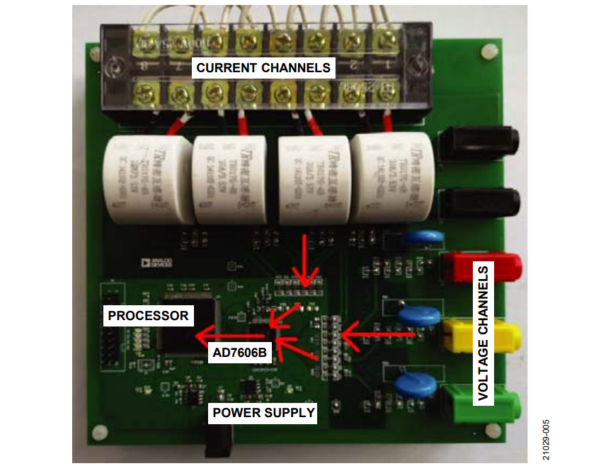
EMC Testing PCB Functions and System Description
The EMC test board has 4× voltage channels that use a resistor divided network to attenuate and measure 100 V ac signals. This circuit is a critical EMC test case because there is no isolation barrier provided by this resistor divided network and the AD7606B input is directly connected to the EMC interference input
The EMC test board also has 4× current channels that use a standard current transformer to sense the 20 A current signal. The current transformer offers an isolation barrier between the system input port and the AD7606B input, which blocks out most of the EMC interference.
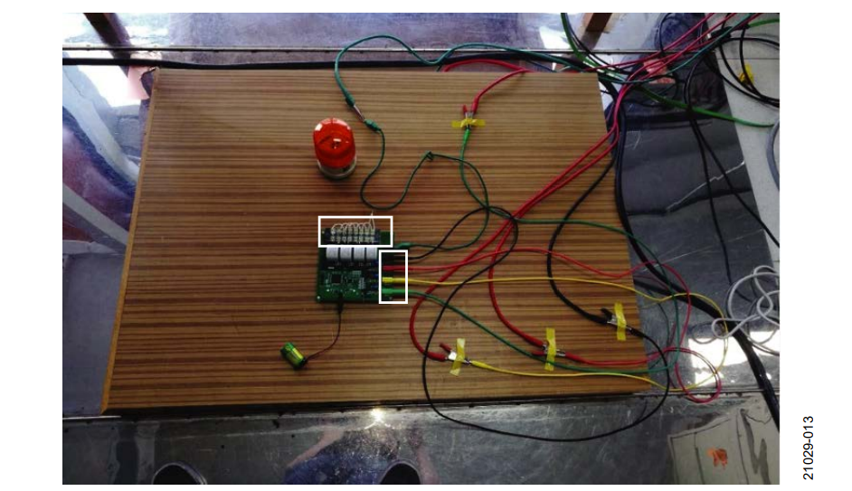
An on-board microprocessor controls sampling and checks the conversion data, timing, and status. If the processor discovers any ADC failures, a failure LED is lit. Based on the color of the failure LED, the user can determine what failure is occurring. If the failure LED does not blink during the test, the AD7606B is robust. Other than the failure LED, an additional LED continuously blinks during testing. This second blinking LED indicates that the processor is working properly.
Analog Input Protection Circuit
Typically, the AD7606B is directly interfaced to the secondary coil of the current transformer. Between the AD7606B input and the secondary coil of the current transformer, there is an RC low-pass filter that reduces high frequency interference from the power grid, attenuates the high frequency EMC interference, and reduces the input overvoltage protection requirement.
A transient voltage suppression (TVS) diode, P6KE6.8C, is placed on the sensor output of the PCB to clamp the overvoltage from the current transformer (see Figure 3). During EMC tests, the TVS is taken off the PCB. The AD7606B still survives the EMC impact, which indicates that the internal overvoltage protection is strong enough to deal with the impact from the secondary coil of the current transformer with the help of the RC low-pass filter.


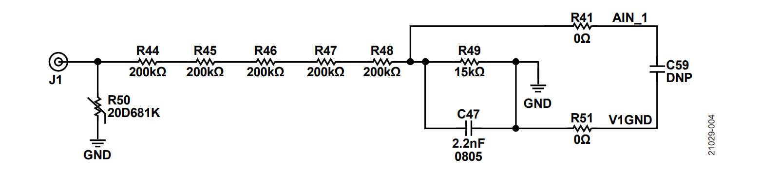
The resistor divider network attenuates the input voltage from 100 V down to the input range of the AD7606B. The resistor R49 (see Figure 5) works with a 2.2 nF capacitor, C47, to build a lowpass filter for signal antialiasing. The same low-pass filter acts as the EMC signal attenuate. The resistor divider network also limits the input current when overvoltage occurs, which protects the AD7606B input.
Additionally, one varistor at each of the voltage channel inputs absorbs voltage surge impacts. Varistors are standard voltage channel EMC protection when the resistor divider network topology is applied.
Circuit Layout Considerations
The following considerations are important for an EMC robust PCB design.
Global Placement

Global placement of the components must follow the signal flow. On the EMC test board, all sensor input ports (voltage input channels and current input channels) are placed on the top and right side of the PCB. The output signals of the sensors are routed to the AD7606B inputs, which sit in the middle of the PCB. The processor connects to the digital side of the AD7606B from the left side of the PCB. Therefore, the global signal flow is from top and right side (sensor input) of the PCB, to the AD7606B in the middle, and then to the processor on the left. This global placement segments the analog high voltage circuit and the digital low voltage circuit on the PCB. If the conductive EMC interference from the analog high voltage area (sensor input) can be blocked or bypassed before flowing to the low voltage digital area, the PCB is EMC safe. A clear segmentation and global signal flow are the preconditions for controlling the conductive interreference on the PCB.

Do Not Use A Split Ground
An analog and digital split ground can improve the SNR performance of the AD7606B, but the risk of an EMC surge is extremely high, especially when a ferrite bead is used to connect the analog and digital grounds together at a single connection point. Figure 6 shows how a split ground can cause an EMC issue.

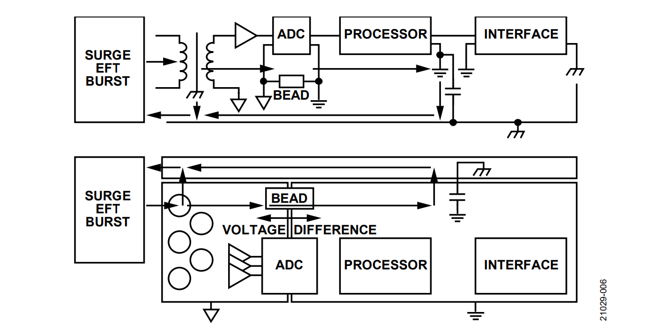
Most EMC interference signals are common mode signals such as EFT/burst. During the common mode EMC test, the EMC signal generator produces a high speed and high voltage interference. The generator then applies the interference between the input port of the device under test (DUT) and the ground.
The common-mode current can be injected into the analog portion of the DUT and enter the analog ground of the PCB via the decoupling capacitor. The common mode current then tries to find a path with the lowest impedance to the earth ground and flows back to the EMC signal generator.
Sometimes, the earth ground of the DUT is near the digital side of the system, which means the common mode current must flow from the analog side to the digital side of the system and then enter the ground. When a split ground is used, the commonmode current must flow through the single connection point between the analog ground and digital ground. This can cause a significant voltage difference between the two ground planes when the current is large enough and can cause the AD7606B to malfunction. Again, this could be extremely critical when a ferrite bead is used to connect the analog and digital ground.
Decoupling Capacitors
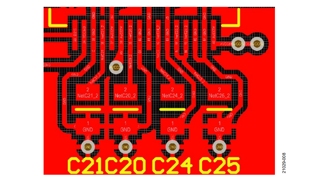
Place the decoupling capacitors near the power supply pins of the AD7606B. The overview of the decoupling capacitors is shown in Figure 7.

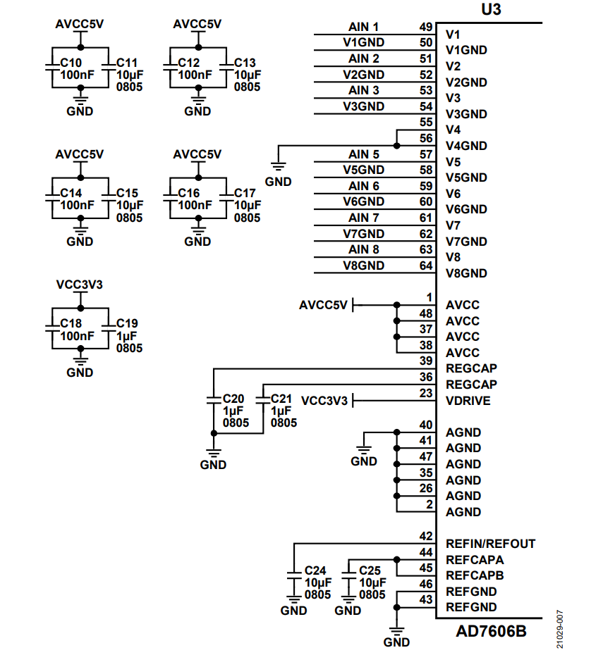
The 1 µF decoupling capacitors for the AD7606B internal voltage regulator are C20 and C21. The 10 µF decoupling capacitors for the voltage reference and reference buffer are C24 and C25. Place these four capacitors on the top layer of the PCB and close to the following pins:
- Connect Pin 35 and Pin 36 to capacitor C21 and keep the trace as short as possible.
- Connect Pin 39 and Pin 40 to capacitor C20 and keep the trace as short as possible.
- Connect Pin 42 and Pin 43 to capacitor C24 and keep the trace as short as possible.
- Connect Pin 44 and Pin 45 together. Connect Pin 46 and Pin 47 together and connect the trace to capacitor C25. Keep the trace as short as possible.

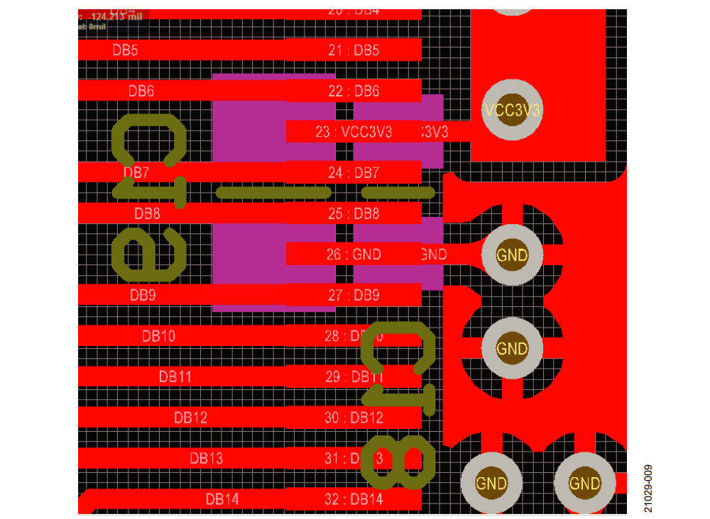
C18 and C19 are the decoupling capacitors for the 3.3 V digital supply. The corresponding pins on the AD7606B are Pin 23 and Pin 26, as shown in Figure 9. Place two vias close to Pin 23 and Pin 26 and place the decoupling capacitors on the bottom layer of the PCB near the vias.

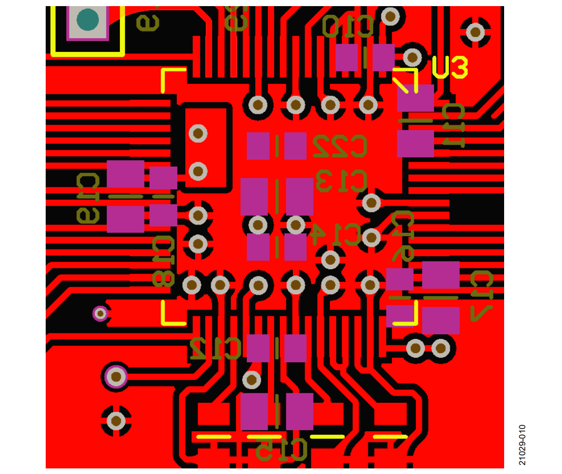
The AD7606B has four 5 V analog supply input pins: Pin 1, Pin 37, Pin 38, and Pin 48. Figure 10 shows the decoupling capacitor placement for those pins. Place the decoupling capacitors (pink footprints in Figure 10) on the bottom side of the PCB near the vias. Keep the trace between vias and the power supply pins as short as possible

EMC Testing
In the following EMC tests, the PCB is powered by a battery.
ESD Testing
Apply a ±8 kV contact discharge and a ±15 kV air discharge interference to the following:
- All voltage channels input ports
- All current channels input ports
- The vertical coupling plane
- The horizontal coupling plane

The LED does not show ADC failure when the previously listed interferences are connected Therefore, the AD7606B passes the system level ESD test.
EFT/Burst Testing
Apply a ±4 kV at 100 kHz interference and a ±4 kV at 5 kHz interference to the following:
- All voltage channels input ports
- All current channels input ports


The LED does not show ADC failure when the previously listed interferences are connected. Therefore, the AD7606B can pass a system level EFT/burst test.
Surge Testing
The AD7606B-based EMC test board has four voltage input channels: Phase A, Phase B, Phase C, and a neutral input, Phase N.
For a common-mode surge test, apply a ±4 kV common-mode voltage between any voltage input and the earth ground, PE. The different connections are:
- Phase A to PE
- Phase B to PE
- Phase C to PE
- Phase A, Phase B, and Phase C to PE
For a differential mode test surge test, apply a ±2 kV differential mode voltage between each voltage input channel. The connections are:
- Phase A to Phase B
- Phase A to Phase C
- Phase A to Phase N
- Phase B to Phase C
- Phase B to Phase N
- Phase C to Phase N

The LED does not show ADC failure when the ±4 kV commonmode voltage or the ±2 kV differential mode voltage is applied to the respective phases. Therefore, the AD7606B can pass the system level surge testing with a proper design.
Authors

