Resource Library
AN-1593: Extending Op Amp Operating Range via Bootstrapping
Abstract
When an off the shelf operational amplifier (op amp) cannot provide the signal swing range needed for a particular application, the engineer is faced with using a high voltage op amp or designing a discrete solution—both choices being potentially costly avenues to solving the problem. A third option, bootstrapping, can be an inexpensive alternative to these approaches for many applications. A bootstrapped power supply circuit involves a fairly straight-forward design exercise in all but the most dynamic performance demanding applications.
The reader is encouraged to read an excellent technical article “Bootstrapping your op amp yields wide voltage swings,” Grayson King and Tim Watkins, EDN Magazine, May 13, 1999 that addresses numerous considerations in bootstrapped amplifier applications.
Introduction to Bootstrapping
A conventional op amp requires its input voltage to be within its power supply rails. In cases where input signals may exceed the supply rails, large inputs can be attenuated resistively to bring these inputs down to a level within the supply range. This case is not ideal because it has adverse effects on input impedance, noise, and drift. These same supply rails limit the amplifier output, which places a limit on the magnitude of the closed loop gain to avoid driving the output into saturation.
Accordingly, if there is a requirement to handle large signal excursions on the input and/or output, wide power supply rails and an amplifier that operates at those rails are needed. Analog Devices, Inc., 220 V ADHV4702-1 is an excellent choice for such situations, although a bootstrapped low voltage op amp may meet the requirements of an application, as well. The decision to bootstrap or not depends primarily on the dynamic requirements and power constraints.
Bootstrapping creates an adaptive dual power supply whose positive and negative voltages are referred to the instantaneous value of the output signal, rather than ground, sometimes called a flying rail configuration. In this arrangement, the supplies move up and down with the output voltage of the op amp (VOUT). Therefore, VOUT is always at midsupply and the supply voltages are able to move relative to ground. Such an adaptive dual supply can be implemented quite easily using bootstrapping.
To be practical, bootstrapping must meet a few criteria—some are trivial but none are particularly onerous. The most basic of these criteria are
- Must not excessively load the output.
- Must respond no slower than the slew rate of the op amp.
- Must handle the voltage levels needed and the associated power dissipation.
Theory of Operation
The flying rail concept is one in which the positive and negative supply rails are continuously adjusted so that their voltages are always situated symmetrically about the output voltage. In this way, the output is always within the supply range.
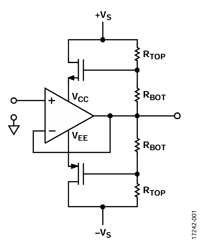
The circuit architecture comprises a complementary pair of discrete transistors and a resistive bias network. An NPN emitter (or source terminal of an N channel MOSFET) provides VCC, and a PNP emitter (or source terminal of a P channel MOSFET) acts as VEE. The transistors are biased such that the desired supply voltages appear at the +VS and −VS pins of the amplifier, with these voltages derived from the high voltage supplies via the resistive dividers. Figure 1 shows a simplified high voltage follower schematic.

In theory, bootstrapping can provide arbitrarily high signal compliance for any op amp. In practicality, the greater the supply scaling, the poorer the dynamic performance becomes because the slew rate of the op amp limits how quickly the supplies can respond to dynamic signals. Operating the amplifier at or near its maximum rated supply voltage minimizes the range that the supply pins need to traverse to keep up with the dynamic signals. When operating the op amp near its highest rated supply voltage, other error sources, such as noise gain, are also reduced (see “Bootstrapping your op amp yields wide voltage swings,” EDN Magazine, May 13, 1999).
Low frequency and dc applications that do not require the supplies to move very far (or very quickly) are the best candidates for bootstrapping. It follows that a high voltage amplifier delivers better dynamic performance than a dynamically equivalent low voltage amplifier, especially when both are biased at their respective maximum operating supply voltages and bootstrapped for the same signal range. Because bootstrapping can also affect dc performance, an op amp optimized for both dc precision and high voltage provides the best combination of dc and ac performance achievable in a bootstrapped configuration.
Design Considerations for a Range Extender Using the Adhv4702-1
The ADHV4702-1 is a precision 220 V op amp. The device eliminates the need to bootstrap traditional low voltage op amps, simplifying high voltage designs in the sub 220 V signal range. If an application calls for a higher voltage, the bootstrapping technique can be applied by easily increasing the operating range of the circuit by more than double. A 500 V amplifier design example based on the ADHV4702-1 follows.
Voltage Range
As discussed, the range of the extender circuit is theoretically unlimited, but some practical limitations include the following:
- Power supply voltage and current rating
- Resistor and field effect transistor (FET) power dissipation
- FET breakdown voltage
DC Bias Level
First, consider the supply voltage provided to the amplifier. Anything in the specified supply range of the device works. However, power dissipation is apportioned between the amplifier and the FETs based on the chosen operating voltage. For a given raw power supply voltage, the lower the op amp supply voltage, the higher the drain source voltage (VDS) in the FETs, with power dissipation also split accordingly. Choose the op amp supply voltage to dissipate power in the components best able to handle heat.
Next, calculate the divider ratio needed to reduce the raw supply voltage (VRAW) to the desired supply voltage of the amplifier (VAMP) by using the following equation:
(VRAW)/(VAMP) = (RTOP + RBOT)/RBOT
where RTOP is top resistor, and RBOT is bottom resistor.
For the following example, consider that the nominal op amp supply voltage is ±100 V. For an application that requires a ±250 V swing range, calculate the application by the following:
Divider Ratio = 250 V/100 V = 2.5, or 2.5:1
Next, design a resistive divider using convenient, standard value resistors that most closely approximate this divider ratio. Keep in mind that the high voltages involved may result in higher resistor power dissipation than might be expected.
Quiescent Power Dissipation
For the chosen resistor values, it is critical to choose resistor sizes that can handle the quiescent power dissipation. Conversely, if the physical sizes of the resistors are constrained, choose their values to limit heat dissipation to within the ratings.
RTOP reaches 150 V and RBOT reaches 100 V in this example. Using Size 2512 resistors rated for ½ watt, the design must limit power dissipation (V2/R) to less than 0.5 W for each resistor. Calculate the minimum value of each resistor as follows:
RTOP = (150 V)2/0.5 W = 45 kΩ minimum
RBOT = (100 V)2/0.5 W = 20 kΩ minimum
Taking the higher value resistor (45 kΩ) as the limiting factor in power dissipation, the RBOT value yielding a 2.5:1 divider while observing quiescent power dissipation limits is
RBOT = RTOP/1.5 = 30 kΩ
which dissipates (100 V)2/30 kΩ = 0.33 W.
Instantaneous Power Dissipation
Considering that the instantaneous voltages of the resistors are dependent on the output voltage of the amplifier as well as the supply voltage, the voltage across each divider at any instant in this example can be as high as 350 V (VCC = 250 V and VOUT = −100 V). A sinusoidal output waveform produces the same average power dissipation in both the VCC and VEE dividers, but any nonzero average output causes more power dissipation in one divider over the other. For a full-scale dc output (or square wave), the instantaneous power is the maximum power.
In this example, to keep instantaneous power below 0.5 W, the sum of the two resistors (RSUM) in each divider must be no less than the following:
RSUM = (350 V)2/0.5 W = 245 kΩ
which, in the resistor ratio of 1.5:1 (for a 2.5:1 divider), makes the minimum values of the individual resistors the following:
- RTOP = 147 kΩ
- RBOT = 98 kΩ
FET Selection
The breakdown voltage required to withstand the worst-case bias conditions primarily drives the choice of FETs, which is seen when the output is saturated, such that one FET is at the maximum VDS and one FET is at the minimum VDS. In the previous example, the highest absolute VDS is ~300 V, which is the total raw supply voltage (500 V) minus the total supply voltage of the amplifier (200 V). Therefore, the FETs must withstand at least 300 V without breakdown.
Power dissipation must be calculated for the worst case VDS and operating current, and FETs must be chosen that are specified to operate at this power level.
Next, consider the gate capacitance of the FET because it creates a low-pass filter with the bias resistors. Higher breakdown FETs tend to have higher gate capacitances, and because the bias resistors tend to be 100 kΩ, it does not take much gate capacitance to considerably slow the circuit down. Obtain the gate capacitance value from the data sheet of the manufacturer and calculate the pole frequency formed with the parallel combination of RTOP and RBOT.
The frequency response of the bias network must remain faster than both the input and output signals, otherwise the output of the amplifier can extend beyond its own supply. The input risks damage from momentary excursions outside the supply rails of the amplifier, whereas the output risks distortion due to momentary saturation or slew limiting. Either of these conditions may result in momentary loss of negative feedback and unpredictable transient behavior, and possibly even latch-up due to phase reversal in some op amp architectures.
Performance
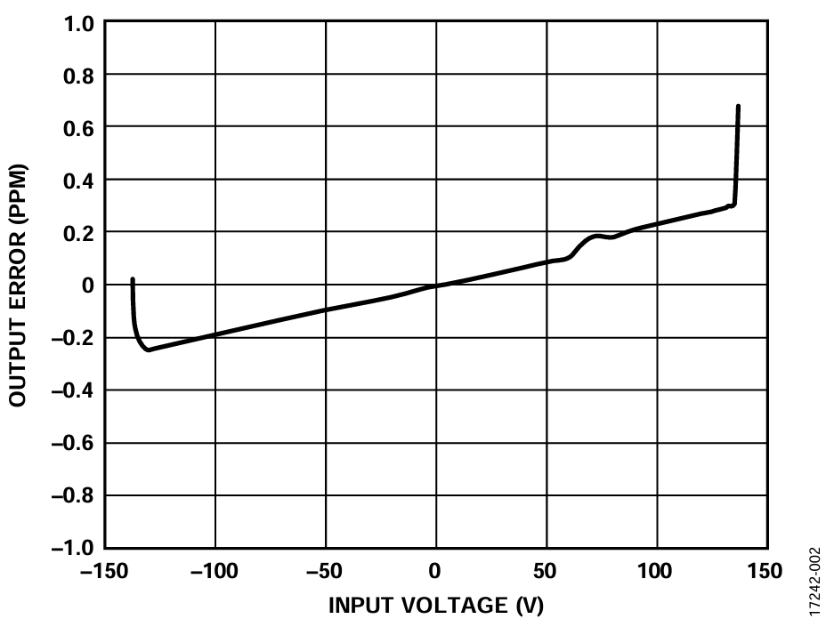
DC Linearity
Figure 2 illustrates gain error as a function of input voltage (dc linearity) in a gain of 20 at a ±140 V supply.

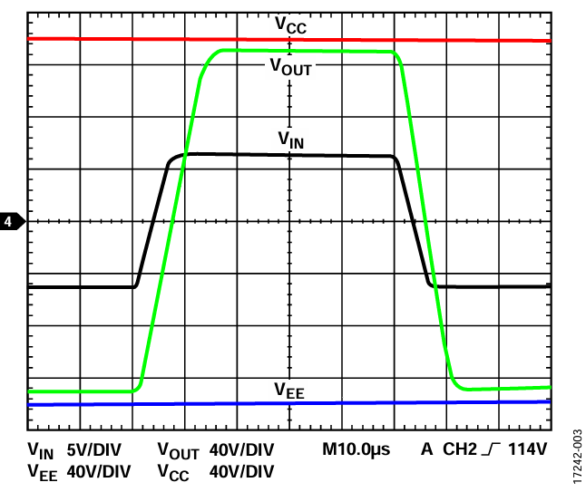
Slew Rate
Figure 3 illustrates the slew rate in a gain of 20 at a ±140 V supply, measured at 20.22 V/μs.

Trade-offs for Higher Speed
Power
As discussed previously, higher working voltages necessitate higher breakdown FETs (with their associated higher gate capacitances) and higher resistor values. Higher resistor and capacitance values both contribute to reducing bandwidth, with the only available adjustment factor being the resistor values. Reducing resistor values increases bandwidth but at the expense of power dissipation.
Space
Lower value and higher power resistors are larger in size and consume more board space.
Adding some lead compensation in the form of a capacitor across RBOT improves the frequency response of the circuit. This capacitor forms a zero with the RBOT and RTOP resistors that counteracts the pole formed by the gate capacitance of the FET. Pole and zero cancellation may permit higher value resistors to be chosen, reducing dc power dissipation.
Conclusion
Conventional op amps are often bootstrapped in applications where higher voltages are required but where typical high voltage op amps are not economical. Bootstrapping has its benefits and drawbacks. Alternatively, the ADHV4702-1 offers a precision, high performance solution up to 220 V without the need for bootstrapping. When signal range requirements exceed 220 V, however, the device can be bootstrapped to handle more than twice its nominal signal range while providing higher performance than a bootstrapped low voltage amplifier.
References
King, Grayson and Watkins, Tim. “Bootstrapping your op amp yields wide voltage swings,” EDN Magazine, May 13, 1999. Wikipedia, “Bootstrapping”, September 1, 2018.