AN-1588: Sensing Low-g Acceleration Using the ADXL345 Digital Accelerometer Connected to the ADuC7024 Precision Analog Microcontroller
AN-1588: Sensing Low-g Acceleration Using the ADXL345 Digital Accelerometer Connected to the ADuC7024 Precision Analog Microcontroller
Circuit Function and Benefits
The ADXL345 is a small, thin, low power, 3-axis accelerometer with high resolution (13-bit) measurement up to ±16 g. Digital output data is formatted as 16-bit twos complement and is accessible through either a serial peripheral interface (SPI), 3-wire or 4-wire, or an I2C digital interface.
The ADXL345 is well suited for mobile device applications. The ADXL345 measures the static acceleration of gravity in tilt sensing applications, as well as dynamic acceleration resulting from motion or shock. The high resolution of the ADXL345 (4 mg/LSB) enables measurement of inclination changes of about 0.25°. Using a digital output accelerometer such as the ADXL345 eliminates the need for analog-to-digital conversion, reducing system cost and real estate. Additionally, the ADXL345 includes a variety of built in features. Activity detection or inactivity detection, tap detection or double tap detection, and free fall detection are all done internally with no need for the host processor to perform any calculations. A built in, 32-stage first in, first out (FIFO) memory buffer reduces the burden on the host processor, allowing algorithm simplification and power savings. Additional system level power savings can be implemented using the built in activity or inactivity detection and by using the ADXL345 as a motion switch to turn the whole system off when no activity is felt and on when activity is sensed again.
The ADXL345 communicates via an I2C interface or an SPI interface. The circuits described in this application note demonstrate how to implement communication via these protocols.

Circuit Description
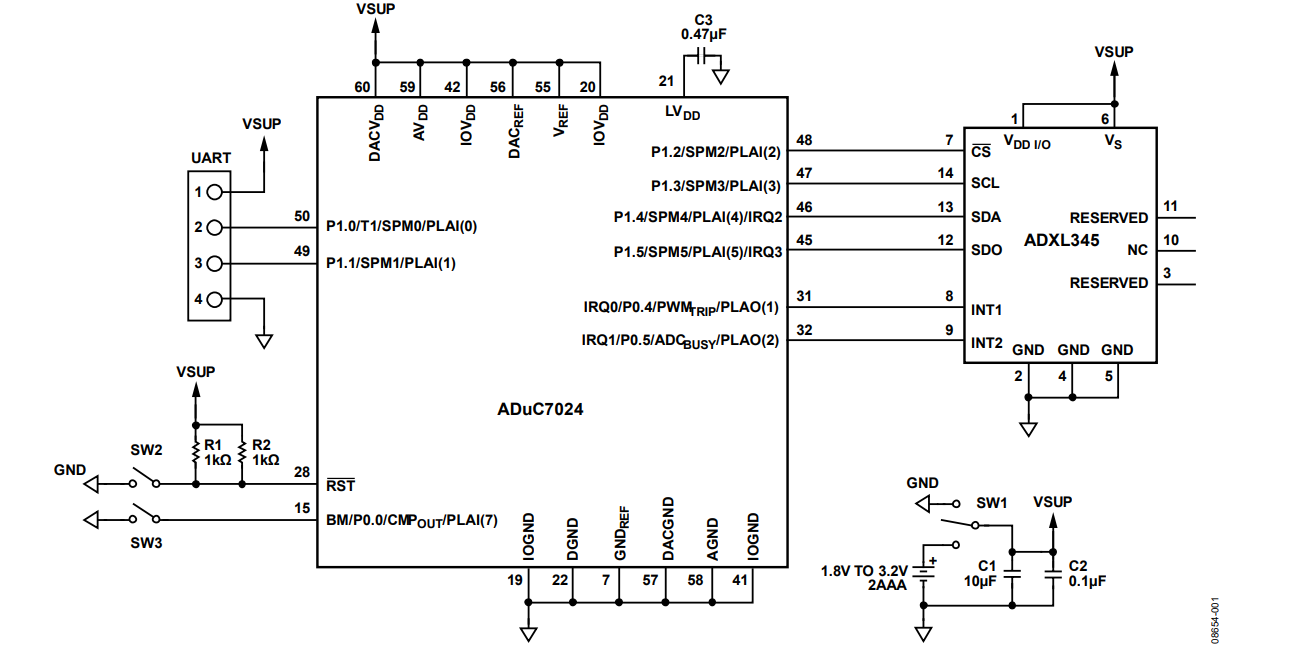
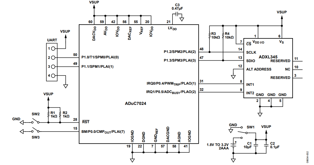
This circuit uses an ADuC7024 precision analog microcontroller in conjunction with the ADXL345 digital accelerometer. Both are I2C ready and SPI ready. Figure 1 shows the ADXL345 and ADuC7024 in an SPI configuration, and Figure 3 shows the same devices in an I2C configuration. The CS pin (Pin 7 on the ADXL345) is used to select the desired interface. I2C mode is enabled if the CS pin is tied high to VDD I/O (Pin 1 on the ADXL345). In SPI mode, CS is toggled to signify the beginning and end of each transmission. Pulling CS high indicates that no SPI transmission is occurring or that an I2C transmission may occur.
Both schematics are simplified but required connections (for example, supplies and ground connections) are shown. In these schematics, the ADuC7024 is programmed via a universal asynchronous receiver-transmitter (UART) that connects to Pin 49 and Pin 50 of the ADuC7024. SW2 and SW3 are reset and download buttons, respectively, for programming the microcontroller. SW1 is an on or off power switch.
Common Variations
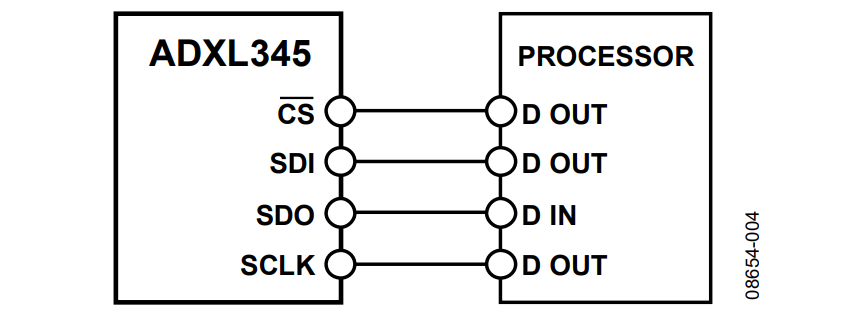
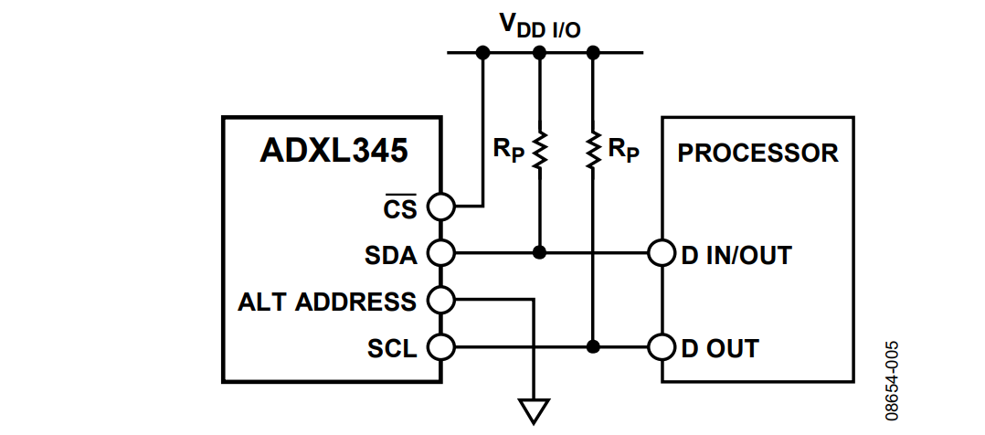
Figure 1 shows the ADXL345 in a 4-wire SPI configuration, and Figure 2 shows that the ADXL345 can also communicate via a 3-wire SPI.


The circuit described in Figure 1 and Figure 3 use the ADuC7024 microcontroller. The same configuration can be applied with any SPI capable or I2C capable microcontroller, as outlined in Figure 4 and Figure 5. The standard I2C connection and SPI connection are used. Pin functions for the two protocols are listed in Table 1.
For information on ADXL345 operation and register functions, refer to the ADXL345 data sheet.
For information on programming the ADuC7024, see the ADuC7024 data sheet.

| Pin Number | Pin Name | Functionality | |
| I2C | SPI | ||
| 7 | CS | Connect to VDD I/O for I2C | Chip select |
| 12 | SDO/ALT ADDRESS | Alternate address select | Serial data output |
| 13 | SDA/SDI/SDIO | Serial data | Serial data input (SPI 4-wire)/serial data input and output (SPI 2-wire) |
| 14 | SCL/SCLK | Serial communications clock | Serial communications clock |