AN-1584: Eight-Pole, Active Low-Pass Filter Optimized for Precision, Low Noise, and High Gain Using the AD8622 and the ADA4062-2 Op Amps
Circuit Function and Benefits
This circuit is a precision, low noise, low power, eight-pole, active low-pass filter with a gain of 40 dB. The circuit uses the Sallen-Key topology with the Butterworth response.
Rather than simply constructing the filter with a quad op amp, the selected combination of dual op amps offers a more optimized solution. The AD8622 low noise (0.2 μV p-p, 0.1 Hz to 10 Hz), low offset voltage (10 μV typical) op amp is used for the input and gain stages. The AD8622 offers low offset voltage and noise for its power (215 μA per amplifier at ±15 V). The ADA4062-2 junction field effect transistor (JFET) input op amp is used for the last two stages and offers low power (165 μA per amplifier). The low input bias current of the ADA4062-2 allows the use of larger resistors and smaller capacitors in the last two stages, thereby reducing the passive component board area.
The filter offers a low power solution (760 μA total quiescent current using ±15 V supplies) that yields not only precision and low noise, but also high gain. Using two dual op amps rather than a single quad op amp also provides flexibility and ease in the printed circuit board (PCB) layout. The ADA4062-2 is also available in a 1.3 mm × 1.6 mm LFCSP. The smaller size is ideal if designers are concerned about board space when using two dual op amps instead of a quad op amp.
Low-pass filters are often used as antialiasing filters in data acquisition systems or as noise filters to limit high frequency noise. The Butterworth filter is a maximally flat magnitude response filter with no ripple in both the pass band and the stop band. However, the Butterworth filter is achieved at the expense of a wider transition band in the frequency response, as compared to other responses that have ripple. Therefore, higher order Butterworth filters are often required. An active filter design is more complex than a passive filter because both the topology and the proper op amps must be selected. However, the active design allows signal gain and eliminates the need for large inductors and capacitors required to implement a low frequency passive filter.
The Sallen-Key topology, also known as the voltage controlled voltage source (VCVS), has been widely used due to its simple design with few circuit elements. The filter shown in Figure 1 has a cutoff frequency (fC) of 10 Hz and overall gain of 100 V/V, or 40 dB. The design can be easily scaled to other frequencies using standard filter design techniques.


Circuit Description
The eight-pole low-pass filter with four complex conjugate pole pairs is implemented by cascading four two-pole Sallen-Key low-pass filters. Section A and Section B are configured as two-pole low-pass filters with a gain of 10 each, while Section C and Section D are configured as unity-gain filters. The arrangement of the cascade is very important. If gain is required, develop the cascade in the early stages to reduce total noise at the output.
To avoid saturation or clipping in the op amps, arrange the stages in order of increasing quality factor (Q). Table 1 shows the Q requirements and pole position associated with each stage of the Butterworth filter. Also, refer to Chapter 8 (Analog Filters) in Linear Circuit Design Handbook for pole locations on the s-plane and Q requirements for filters of a different order of stages.
| Sections | Poles | Q |
| A | −0.9808 ± imaginary number (j) 0.1951 | 0.5098 |
| B | −0.8315 ± j 0.5556 | 0.6013 |
| C | −0.5556 ± j 0.8315 | 0.9000 |
| D | −0.1951 ± j 0.9808 | 2.5628 |
To reduce cost and board space, a quad amplifier is generally used to implement an eight-pole filter. However, consider using two dual op amps instead of a quad op amp because of the added benefits. With two dual op amps, PCB layout is easier, and the number of board layers can sometimes be reduced. Traces can be spread out, thereby reducing parasitic capacitances and crosstalk. With different gain, bandwidth, noise, and dc precision requirements for each stage, it is important to choose the appropriate amplifier for each stage of the filter.
Use a low noise and low offset voltage op amp for the first stage of the filter because noise and offset from the first stage is multiplied by the noise gain of all four stages. The AD8622 is a dual, low power, precision op amp. At supply voltages of ±15 V, the 0.1 Hz to 10 Hz voltage noise is 0.2 μV p-p, and the typical offset voltage is only 10 μV. The dc precision and low noise of the AD8622 makes this device a good choice for the first two stages of the filter. Smaller resistors are chosen for the first two stages to reduce their thermal noise contribution to the overall noise of the filter. When the total filter gain occurs in the first two stages, the noise requirement for op amps in the remaining stages is not as important. Therefore, the last two stages of the filter are lower cost and less precise.
The low power ADA4062-2 is selected for Section C and Section D. The ADA4062-2 has JFET differential pair inputs with high input impedance and very low bias current. Because the noise requirement is reduced for the last two stages, and the ADA4062-2 has very low bias current, larger resistor values can be used with smaller capacitors. The low input bias currents of the JFETs contribute minimal dc errors to the circuit.
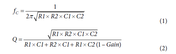
Calculate the fC and Q for an individual two-pole low-pass filter with the following equations:
As a general rule, choose the gain bandwidth product of the op amp that is at least 100 times greater than the product of the fC, Q, and gain of the filter for the equations to be accurate.
For sufficient full power bandwidth, slew rate is also a concern. Slew rate is given by the following general equation:
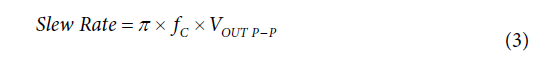
For a 10 Hz fC, the AD8622 and ADA4062-2 both have sufficient slew rates to avoid slew rate limiting.
It is also important to choose appropriate resistor and capacitor values. Selecting a large resistor causes an increase in thermal noise. Although smaller capacitors can then be used to achieve a particular fC, the input capacitance of the amplifier may then be significant. The capacitors are at least 100 times greater than the input capacitance of the amplifiers. The resistors and capacitors are very important in determining the performance over manufacturing tolerances, time, and temperature. At least 1% or better tolerance resistors and 5% or better tolerance capacitors are recommended. Bypass capacitors (not shown in Figure 1) are also needed. In this case, place a 10 μF tantalum capacitor in parallel with a 0.1 μF ceramic capacitor on each power pin of each dual op amp. Details of proper decoupling techniques can be found in Tutorial MT-101.
Figure 2 shows the actual measured frequency response of the low-pass filter. The output from each stage, outlined in the following list, is shown in Figure 2.


- V1 is the output of the first stage.
- V2 is the output of the second stage.
- V3 is the output of the third stage.
- VOUT is the final filter output.
V1 shows a 40 dB/decade roll-off. V2 shows an 80 dB/decade roll-off. V3 shows a 120 dB/decade roll-off. The desired output at VOUT shows a 160 dB/decade roll-off with a sharp transition band. The transition band becomes sharper as the order of the filter increases.
Analog Devices, Inc., has a Filter Wizard design tool that helps users not only design the active filter, but also select the appropriate op amp. The tool guides users through the filter application design process. These steps include entering filter criteria, reviewing recommended devices, active filter synthesis, and, finally, generating a bill of materials and/or the op amp simulation program with integrated circuit emphasis (SPICE) netlist.
References
Rich, Alan. AN-347 Application Note. Shielding and Guarding. Analog Devices.