AN-1397: Using the ADM3065E 50 Mbps RS-485 Transceiver in EnDat Motor Control Encoder Applications
AN-1397: Using the ADM3065E 50 Mbps RS-485 Transceiver in EnDat Motor Control Encoder Applications
Introduction
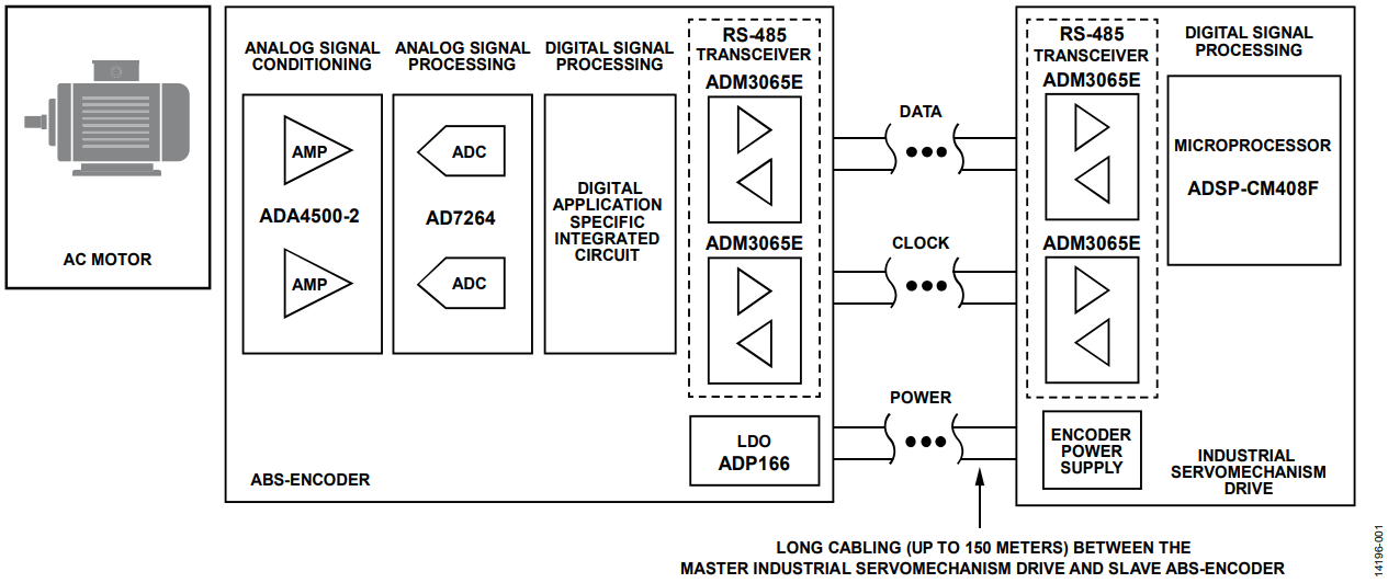
Motor position and angle encoders, also known as absolute encoders, are commonly used in systems with servomechanism drives, robotics, machine tools, and elevators. Figure 1 shows a motor control signal chain, using RS-485 transceivers to interface between the absolute encoder (ABS encoder) slave and industrial servomechanism drive master for closed-loop control of an ac motor. The ABS encoder translates mechanical motion (position and direction) into electrical signals, which are fed back to the servomechanism drive. The servomechanism drive provides intelligent control of the ac motor based on the encoder information. The RS-485 communication link between the servomechanism drive and ABS encoder typically requires high data rates, up to 16 MHz, and low propagation delay timing specifications. The RS-485 cabling typically extends to a maximum of 50 meters, but in some cases can be as long as 150 meters. In harsh industrial environments, the exposed cable and RS-485 connectors can be exposed to harmful electromagnetic current (EMC) events, such as international electrotechnical commission (IEC) 61000-4-2 electrostatic discharges (ESD).

RS-485 for EnDat Encoders
This application note illustrates the benefits for EnDat motor control encoder applications using the Analog Devices, Inc. ADM3065E 50 Mbps (25 MHz) RS-485 transceiver. The ADM3065E transceiver is designed for reliable operation in harsh motor drive or encoder environments, with added noise immunity and IEC 61000-4-2 ESD robustness as key features. The ADM3065E timing specifications, in particular, the low driver and receiver propagation delay, reduce system design complexity for industrial servomechanism drive to ABS encoders. The low propagation delay helps to reduce system design complexity for all system clock frequencies, not only at the high end (16 MHz) for EnDat encoders. Key benefits for motor control applications are illustrated in this application note using relevant application circuits and timing measurements.
RS-485 Ruggedness for Encoders
Motor control encoder applications are challenging environments for data communications, because electrical noise and long cable lengths affect the stability of ABS encoder to servomechanism drive RS-485 signaling. Analog Devices RS-485 transceivers are designed for reliable operation in these harsh environments, with added noise immunity and robustness.
Noise Immunity
RS-485 signaling is balanced, differential, and inherently noise immune. System noise couples equally to each wire in an RS-485 twisted pair cable. One signal emits the opposite of the other signal, and electromagnetic fields coupled onto the RS-485 bus cancel each other out. This reduces the electromagnetic interference (EMI) of the system. In addition, the enhanced ADM3065E 2.1 V drive strength allows greater signal-to-noise ratio (SNR) in communications.
The RS-485 receiver hysteresis also improves noise immunity and is explained further in the Enhanced RS-485 Transceiver Performance section. Adding Analog Devices iCoupler® technology further boosts noise immunity.
Enhanced RS-485 Transceiver Performance
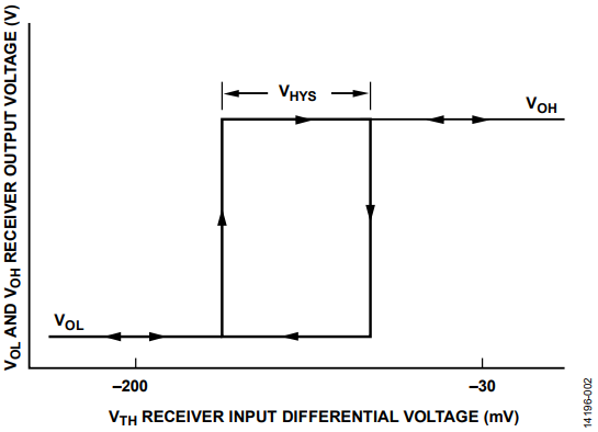
The TIA/EIA-845-A RS-485 standard suggests that RS-485 transceivers implement measures to prevent instability or oscillatory conditions in the receiver device. Receiver hysteresis helps to improve receiver stability and provides a measure of noise immunity, especially important for cables running through harsh industrial motor control environments.
The ADM3065E data sheet specifies a typical receiver hysteresis (VHYS) of 30 mV, with receiver differential input threshold voltage (VTH) of −200 mV to −30 mV.
The VTH is the threshold for the receiver output (VOL and VOH) to change from high to low, or low to high. The VHYS is essentially the difference between VTH for high to low (left-hand side in Figure 2), and VTH for low to high (right-hand side in Figure 2). The VHYS helps to ensure that noise around VTH does not result in spurious logic high and low transitions on the receiver output.

Adding Signal Isolation for Increased Noise Immunity
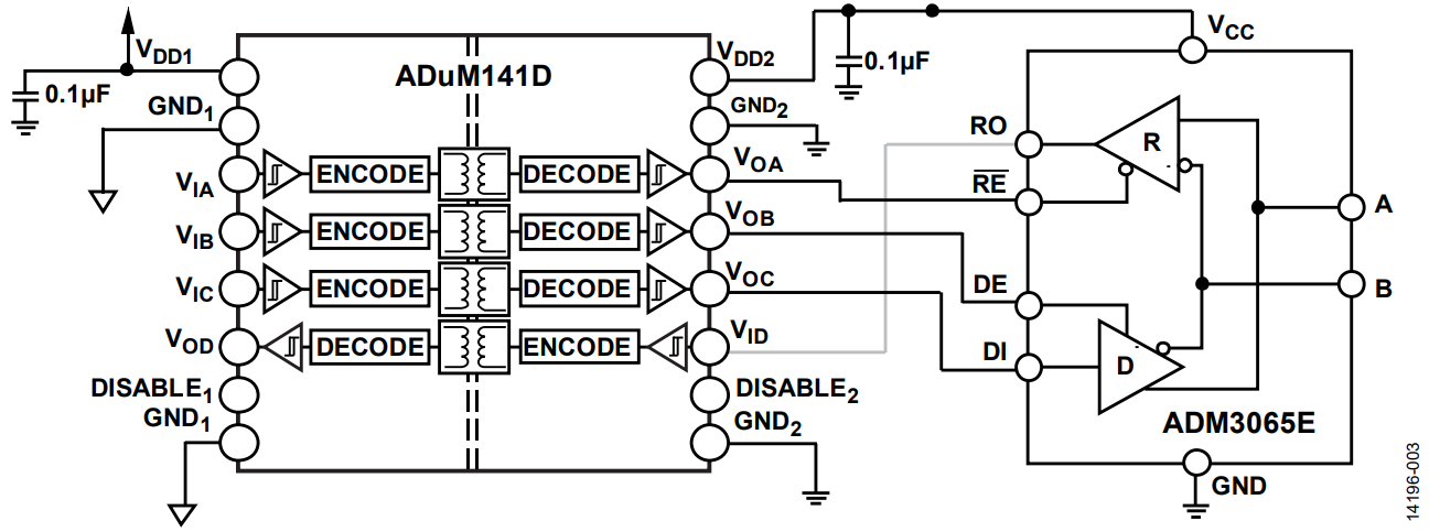
Adding signal isolation to the ADM3065E can be easily implemented using the ADuM141D. The ADuM141D is a quad-channel, digital isolator based on Analog Devices iCoupler® technology. The ADuM141D can operate at a data rate of up to 150 Mbps, making it suitable for operation with the 50 Mbps ADM3065E RS-485 transceiver (see Figure 3).

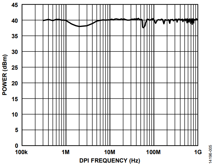
Direct power injection (DPI) measures the ability of a device to reject noise that is injected into the power supply or input pins. The isolation technology used in the ADuM141D has been tested to the DPI IEC 62132-4 standard. The ADuM141D was tested to the DPI IEC 62132-4 standard, with a high power noise source capacitively coupled into either the VDD1 or VDD2 power supply pin. The noise source was swept through a 300 kHz to 1 GHz frequency band. During DPI IEC 62132-4 testing, the ADuM141D VIA pin was clocked, with the clock data monitored for errors (loopback test mode). The fail criteria was defined as greater than ±10% change in the bit width of the signal. Figure 4 shows an example test setup, with the DPI noise source injected through a 6.8 nF capacitor on the ADuM141D VDD1 power supply pin.

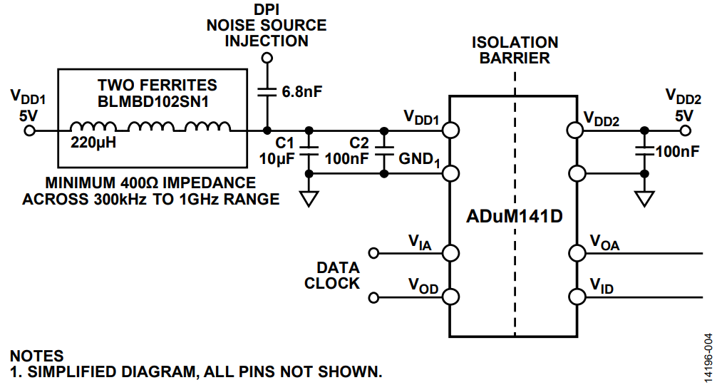
Figure 5 is a typical performance plot showing the fail point for the ADuM141D across noise power (dBm) vs. DPI frequency (Hz). Performance to the IEC 62132-4 standard was evaluated for the ADuM141D and compared to other isolators available in the market. The ADuM141D noise immunity performance exceeds that of similar products. The ADuM141D maintains excellent performance over frequency, but other isolation products exhibit bit errors in the 200 MHz to 700 MHz frequency band (see Figure 5).

Robustness and Reliability
The ADM3065E offers high temperature capability with reliable operation at up to +125°C ambient temperatures, and enhanced RS-485 performance over a wide power supply operating range of 3.0 V to 5.5 V. This provides a reliable flexible solution for encoders and motor drives with different power requirements.
Bus Idle, Open, and Short Circuit Fail-Safe
The ADM3065E features a fail-safe RS-485 receiver, which can help detect unconnected cables on the ABS encoder to the servomechanism drive RS-485 interface.
The ADM3065E has a true fail-safe feature, offering a logic high receiver output feature for bus idle, open, and short circuit across the entire receiver input common mode range of −7 V to +12 V. Figure 6 compares the ADM3065E and a standard RS-485 transceiver on metrics of receiver input threshold voltage and receiver output logic. The ADM3065E features a logic high output for receiver input threshold voltages greater than −30 mV, compared to the standard RS-485 +200 mV.

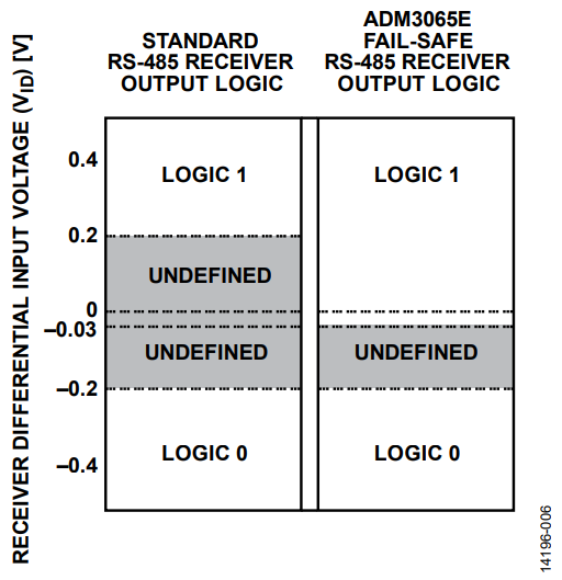
The open circuit fail-safe ensures that the ADM3065E receiver output is high when the RS-485 A pin and B pin are disconnected, with no termination resistor or other nodes present. This feature is present on all Analog Devices RS-485 transceivers. There is an internal pull-up resistor on the ADM3065E A pin. If the A pin is disconnected and floating, then the pull-up resistor pulls the A pin to > −30 mV. There is a pull-down resistor on the ADM3065E B pin. If the B pin is disconnected and floating, then this pull-down resistor pulls the B pin to less than −200 mV. In this scenario, the A pin voltage is greater than the B pin voltage, which creates a bus differential voltage high, and the receiver output logic is a constant high.
The short-circuit fail-safe ensures the ADM3065E receiver output is high when two nodes are driving the bus to opposite levels, or when the bus lines are shorted together.
The bus idle fail-safe is more complex that the bus open/bus short-circuit fail-safe described in this section, and provides a logic high ADM3065E receiver output when no node is driving a signal on the RS-485 bus. There are two main methods of providing this fail-safe. The first is a fail-safe RS-485 transceiver that has an offset receiver threshold, for example, −30 mV rather than the TIA/EIA-845-A RS-485 standard +200 mV. Analog Devices RS-485 transceivers with bus idle fail-safe also have short-circuit fail-safe. The second method is to use pull-up and pull-down resistors on the bus to ensure a minimum differential voltage. This method is also called active or powered termination. The required resistor value can be calculated based on the supply voltage and bus load, including termination resistors and receiver impedances.
IEC 61000-4-2 ESD Performance
ESD on the exposed RS-485 connectors and cabling for the encoder to motor drive is a common system hazard. The system level IEC 61800-3 standard relating to EMC immunity requirements for adjustable speed, electrical power drive systems requires a minimum ±4 kV contact/±8 kV air IEC 61000-4-2 ESD protection. The ADM3065E exceeds this requirement with ±12 kV contact/±12 kV air IEC 61000-4-2 ESD protection.
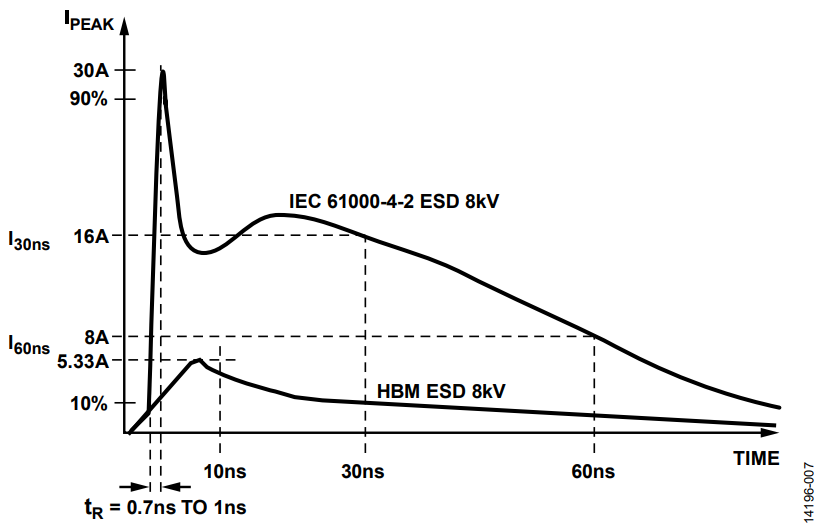
Figure 7 shows the 8 kV contact discharge current waveform from the IEC 61000-4-2 standard compared to the human body model (HBM) ESD 8 kV waveform. Figure 7 shows that the two standards specify a different waveform shape and peak current from one another. The peak current associated with an IEC 61000-4-2 8 kV pulse is 30 A, while the corresponding peak current for the HBM ESD is more than 5× less, at 5.33 A. The other difference is the rise time of the initial voltage spike, with IEC 61000-4-2 ESD having a much faster rise time of 1 ns, compared to the 10 ns associated with the HBM ESD waveform. The amount of power associated with an IEC ESD waveform is much greater than that of an HBM ESD waveform. The HBM ESD standard requires the equipment under test (EUT) to be subjected to three positive and there negative discharges, while in comparison the IEC ESD standard requires 10 positive and 10 negative discharge tests.
The ADM3065E with the IEC 61000-4-2 ESD ratings is suited for operation in harsh environments compared to other RS-485 transceivers that state varying levels of HBM ESD protection.

Glitch Free Power-Up/Power-Down
The ADM3065E features a comprehensive glitch free power-up/ power-down (hot swap) protection.
When a circuit board is inserted into a powered (or hot) backplane, differential disturbances to the data bus can lead to data errors. During this period, processor logic output drivers are high impedance and are unable to drive the DE and RE inputs of the RS-485 transceivers to a defined logic level. Leakage currents up to ±10 µA from the high impedance state of the processor logic drivers can cause standard complementary metal-oxide semiconductor (CMOS) enable inputs of a transceiver to drift to an incorrect logic level. Additionally, parasitic circuit board capacitance can cause coupling of the VCC pin or the GND pin to the enable inputs. Without the hot swap capability, these factors can improperly enable the driver or receiver of the transceiver. When the VCC power supply rises, an internal pull-down circuit holds the DE pin low and the RE pin high. After the initial power-up sequence, the pull-down circuit becomes transparent, resetting the hot swap tolerable input.
Superior RS-485 Timing Performance
Signaling Rate
The ADM3065E provides compliance to high data rates required in BiSS, EnDat 2.2, and HIPERFACE DSL® encoder standards. For encoder standards that use RS-422 transceivers, such as serial synchronous interface (SSI), the ADM4168E transceiver offers a reliable low and high data rate solution. Table 1 provides a number of half and full duplex options for the listed encoder standards.
Table 1. ADI Transceiver Solutions for Motor Control Absolute Encoder Interfaces
| Encoder Standard | Physical Layer | Data Rate (MHz) | High Data Rate RS-485 Transceiver Options | Low Data Rate RS-485 Transceiver Options |
| EnDat 2.2 | RS-485 | 0.1 to 16 | ADM3065E, ADM3066E | ADM3061E, ADM3062E |
| BiSS | RS-422 | 0.08 to 10 | ADM4168E, ADM3067E | ADM4168E |
| HIPERFACE DSL | RS-485 | 4.69 | ADM3065E, ADM3066E | ADM3061E, ADM3062E |
| SSI | RS-422 | 2 | ADM4168E, ADM3067E | ADM4168E |
| EnDat 2.1 | RS-485 | 0.1 to 2 | ADM3065E, ADM3066E | ADM3061E, ADM3062E |
EnDat Encoder Interfaces
Rotary encoders are widely used in industrial automation systems. A typical use of this type of encoder is for electric machines where the encoder is connected to the rotating shaft and thereby provides feedback for the control system. While the primary purpose of the encoder is angular position and speed measurement, additional features, such as system diagnostics and parameter configuration are common as well. This section discusses implementation and testing of the master side of the interface between the encoder and the controller.
Communication Protocols
The communication between the encoder (slave) and the controller (master) is a digital, bidirectional pipe with the robustness to work in an industrial environment as well as the speed to operate in a real-time control system.
Some communication protocols are open-source, but some drive manufacturers choose to define their own protocols. In total, more than 20 different protocols exist. The EnDat and BiSS protocols are examples of two prominent protocols.
Despite their differences, the encoder communication protocols have similarities in regard to implementation. The interfaces of these protocols are serial, bidirectional pipes that comply with either the RS-422 or RS-485 electrical specifications. The data across the links are transmitted in synchronism with the clock provided by the master. Several types of data are exchanged across the link (for example, position values, parameters, and diagnostics) with the type selected through commands sent from the master to the slave.
While there are commonalties in the hardware layer, the software required to run each of the protocol is unique. Both the communication stack and the required application code are specific to the protocol.
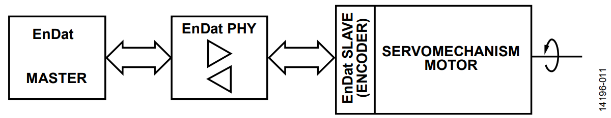
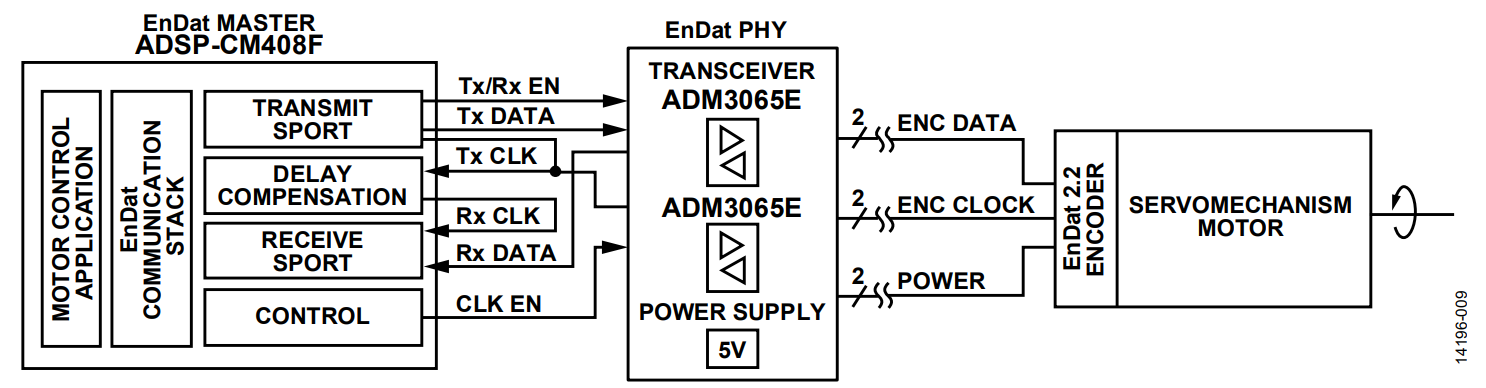
This application note focuses on hardware and software implementation of the master side of an EnDat 2.2 interface, as shown in Figure 8.

Impact from Delays
In some industrial applications, the controller and the encoder are physically separated by more than 100 meters. When this distance is combined with communication speeds of up to 16 MHz, the sensitivity of the system to delay transport is clear.
Delays fall into two categories. First, there is the transport delay of the cable (tCABLE). Second, there is the propagation delay of the transceivers (tTRX). The total delay, (tDELAY), is the sum of the two:
tDELAY = tCABLE + tTRX
The speed of light and the dielectric constant of the cable determines cable delay with typical numbers of 6 ns/m to 10 ns/m. With short cables, this delay is less of an issue but becomes a factor as the cable gets longer.
The master supplies the clock which then travels down the cable and at the encoder the clock is delayed by the full length of cable. The slave transmits the data and the data travels back along the cable using this clock. This means that the data received by the master are delayed by 2× the cable length.
The second source of delay is the propagation delay of the transceivers. Assuming there are transceivers on both the master and slave side, and that data travel down and back the cable, the signals get delayed by four transceivers. This cable length and number of transceivers indicates why propagation delay is an important parameter that must be considered.
The user cannot influence the cable length because it is determined by the physical distance between the master and the slave. However, the user can influence the propagation delay through the selection of the transceivers.
Delay Compensation
When tDELAY exceeds half a clock period, the communication between the master and the slave breaks down. At this point, the designer has the following options:
- Lower the data rate.
- Bring down the propagation delay of the transceivers.
- Introduce delay compensation on the master side.
Option 3 compensates for both cable delay and transceiver delay and therefore is an effective way to ensure that the system can run with high clock rates on long cables. The disadvantage to using Option 3 is that the delay compensation increases the complexity of the system and may not be supported by the master.
In systems where delay compensations are either not possible, or in systems with short cables, the value of using transceivers with a short propagation delay is evident. A low propagation delay enables a higher clock rate without having to introduce delay compensation in the system.
Note that the value of low propagation delay is not only present at high data rates. Systems without delay compensations typically run at lower data rates, which is another benefit of having low propagation delay.
Master Implemenation
Regardless of the protocol, a master implementation consists of a serial port and a communication stack. Because the encoder protocols do not comply with standard ports, such as a serial peripheral interface (SPI) or a universal asynchronous receiver/ transmitter (UART), the peripherals found on general-purpose microcontrollers cannot be used. Instead, it is typical for users to use field-programmable gate arrays (FPGAs) to implement the encoder interface. The programmable logic of an FPGA enables implementation of dedicated communication ports in hardware and support of advanced features such as delay compensation. The communication stack is suited to software implementation, and it is common to have the communication stack running on a processor.
While an FPGA approach is flexible and can be tailored to the application, it also comes with disadvantages. First, an FPGA is expensive when compared to a processor. Second, an FPGA is power hungry. Finally, the development time needed to design a custom FPGA is significant and not always acceptable when considering time to market.
The implementation of the EnDat interface discussed in this application note is done on the ADSP-CM408CSWZ-AF which is a standard processor targeting motor control drives. Besides peripherals for motor control, such as pulse width modulator (PWM) timers, analog-to-digital converters (ADCs), and SINC filters, the ADSP-CM408CSWZ-AF has highly flexible serial ports (SPORTs). These SPORTs are capable of emulating a number of protocols, including encoder protocols such as EnDat and BiSS.
Because of the rich peripheral set of the ADSP-CM408CSWZAF, it is possible to perform advanced motor control as well as interfacing to an encoder with the same device. In other words, the need for an FPGA is eliminated. The user does not have to develop a hardware description language (HDL) code for the FPGA and can focus on C-code and standard processor development tools. In addition, there are savings in PCB area and a processor typically requires less power to run than an FPGA.
Test Setup
An EnDat 2.2 application setup is shown in Figure 9. The EnDat slave is a standard servomechanism motor from Kollmorgen® (AKM22) with an EnDat encoder (ENC1113) mounted to the shaft. Three pairs of wires (data, clock, and power lines) connect the encoder to the transceiver board. There are two transceivers (ADM3065E) and power supply for the encoder on the EnDat PHY. One of the transceivers is used for the clock, and because the clock is always provided by the master, this data flow is unidirectional. The other transceiver is used for the data line. The data line is half-duplex and the data flow is bidirectional.
The EnDat master is realized with ADSP-CM408CSWZ-AF using a mix of standard peripherals and software. Both the transmit port and receive port are implemented with flexible SPORTs. These SPORTs handle all tasks related to the communication: shifting data in and out, generating the clock signal to the EnDat slave, and providing control signals for the transceivers.
As discussed in the Impact from Delays section, long cables introduce delays, which means that the data received from the slave are out of phase with the clock provided by the master. An effective way to compensate for the cable delay is to phase shift the clock used on the receiving SPORT (see Figure 9). For this setup to work, the phase shift of the clock must match the total delay of the system.

Using direct memory access (DMA), data are transferred between the peripherals of the ADSP-CM408CSWZ-AF and the communication stack. This minimizes the software overhead associated with communication. The stack handles tasks such as sequencing, sending commands to the encoder, and receiving data from the encoder. The data from the encoder are presented to the motor control application, which also runs on the ADSPCM408CSWZ-AF.
EnDat Protocol
The EnDat protocol consists of a number of different frames of varying length, however, these frames are all based on the same sequence. First, the master issues a command to the slave, then the slave processes the command and performs the necessary calculations. Finally, the slave sends the result back to the master. Figure 10 shows an example of the communication between master and slave.

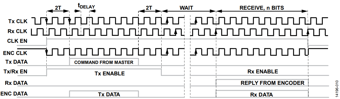
In Figure 10, the transceiver clock (Tx CLK) is the transmit clock generated by the ADSP-CM408CSWZ-AF This is the clock supplied to the encoder but because of the cable length and other delays in the system, the data from the encoder will be out of phase with the Tx CLK before they get back to the ADSPCM408CSWZ-AF. To compensate for transport delay, tDELAY, the ADSP-CM408CSWZ-AF also issues a receive clock (Rx CLK) signal, which is delayed by tDELAY compared to the Tx CLK. Bringing the Rx CLK in phase with the data received from the slave is an effective way to compensate for the transport delay.
The clock signals from the ADSP-CM408CSWZ-AF are continuous while the EnDat protocol specifies the clock must only be applied to the encoder during communication. At all other times the clock line must be held high. To handle this clock signal, a clock enable signal, CLK EN, is fed to the ADM3065E data enable pin. CLK EN is generated by the ADSP-CM408CSWZ-AF and is synchronized to the transmit clock. The encoder sees the clock signal, ENC CLK.
After exactly two clock periods, 2T, the master starts clocking out the command on transceiver data. The command is 6 bits long and is followed by two 0 bit. To control the data direction through the data transceiver, the ADSP-CM408CSWZ-AF sets Bit Tx EN and Bit Rx EN high while transmitting. This signal is fed to the ADM3065E receive enable (RE) pins and data enable (DE) pins. Note that ADM3065E is kept in either transmit or receive mode and never fully disabled. Switching between Tx or Rx mode happens with short delay while switching from disabled mode to enabled mode takes considerably longer.
After sending the command, the slave prepares a response. The length of time required to get a response ready depends on the type of command and the type of encoder.
Therefore, the system enters a wait state where the master continues to apply clocks but the data line is inactive. When the slave is ready to respond, the data line, Rx data, is pulled high and the response is sent immediately after. After receiving the n bits response, the master stops the clock by setting CLK EN signal low. At the same time, the ENC CLK signal goes high.
As mentioned, the data flow is half-duplex and the traffic on the combined data line is shown as ENC data.
Figure 10 shows that the Tx CLK and Rx data are out of phase because of the transport delay. Delaying Rx CLK by tDELAY brings the receive clock and Rx data in phase.
Synchronization
One of the advantages of having the motor control application and the encoder interface running on the same device is a tight synchronization. In a motor control loop, it is desirable to synchronize current measurement and position feedback to the PWM pattern applied to the power inverter. With the ADSPCM408CSWZ-AF, this synchronization is realized using a combination of triggers and DMA, as shown in Figure 11. When a new PWM period is initiated, the PWM timer generates a synchronizing pulse, PWM_SYNC. This pulse triggers current measurement (not shown) and it triggers a DMA transfer of data from the memory to the transmit port. The data is a command to the encoder, for example, send position.

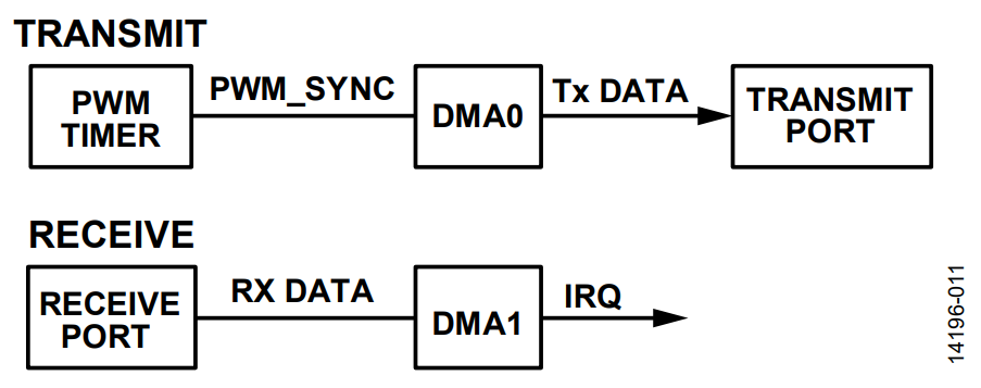
When the encoder is ready to send data back to the master, the receive port captures the data and DMA transfers the result to memory. An interrupt, IRQ, notifies the communication stack that the data are ready to be processed. This process occurs without any software interaction, resulting in an efficient implementation.
Experimental Results
Figure 12 and Figure 13 show test results from the EnDat system discussed throughout this application note. The clock frequency used in the test is 8 MHz, and the delay compensation is achieved by phase shifting the receive clock.
In Figure 12 , the bottom signal is the command from the EnDat master. The command shown here is send position, which is two 0s, followed by six 1s, and ended with another two 0s. In total, the command is 10 bit long. The response from the encoder is the third signal from the top. This signal is measured at the receiver output pin, RO, of the ADM3065E and is therefore single-ended. The combined data line is the second signal from the top. This measurement is the difference between the A pin and the B pin of the ADM3065E and the signal is differential. Finally, the top signal is the clock applied to the encoder.

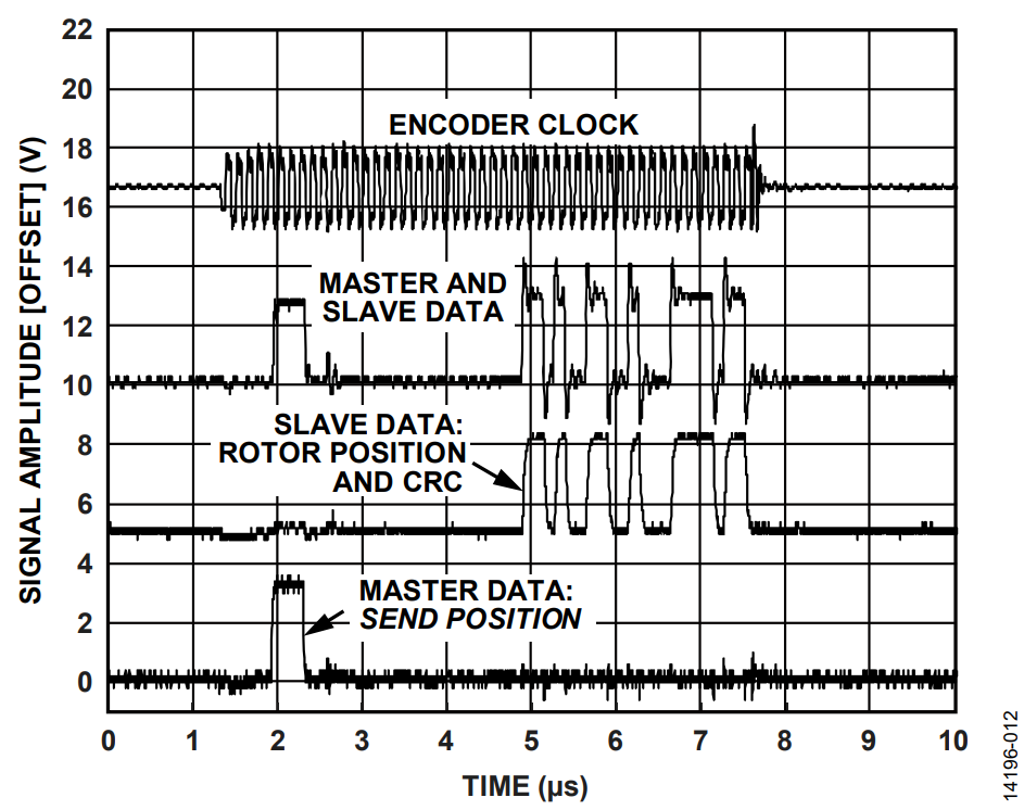
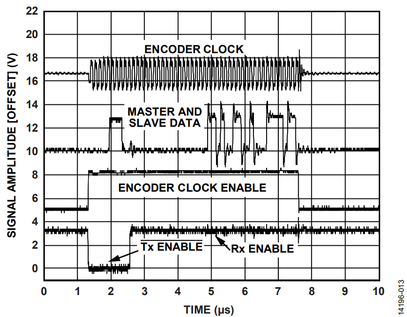
Figure 13 illustrates the control lines for the ADM3065E during a transmit and receive sequence. The bottom signal shows the data enable and receive enable signal for the transceiver handling data. Low indicates transmit and high indicates receive. The third signal from the top shows the data enable signal for the transceiver handling the clock. When the signal is high, the encoder clock signal is applied to the encoder. The master and slave data signal is the combined data line. After data from the encoder have been received by the ADSP-CM408CSWZ-AF, an interrupt is generated and the EnDat stack is executed.

Authors

