AN-1347: Operating the ADF4360-7 at High PFD Frequencies
Introduction
The ADF4360-7 is a very flexible synthesizer (phase-locked loop (PLL) with an integrated voltage controlled oscillator (VCO)) that enables the generation of frequencies from 350 MHz to 1800 MHz. An on-chip calibration engine fine tunes the output frequency after power-on. Under most operating conditions, the calibration process works well; however, timing uncertainty errors can occur, which result in tuning errors that degrade the phase noise and/or spurious performance. This application note describes how to maintain optimum performance when operating the device at a relatively high phase frequency detector (PFD) frequency.
Background
RF designers often want to maximize the PFD frequency for improved phase noise performance. In most cases, maximizing the PFD frequency is desirable; however, it can lead to the ADF4360-7 operating outside its specified operating parameters.
Figure 1 shows a block diagram of the ADF4360-7. The reference input, REFIN, is divided by the 14-bit R counter producing the PFD frequency. The output of the VCO is fed back to the N counter, dividing it down. The outputs of the R and N counters go to the phase comparator. The PLL closes the loop by driving the phase error to zero.

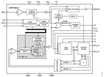
Figure 1. ADF4360-7 block diagram.
The Analog Devices, Inc., PLL simulation software ADIsimPLL generates the R and N register values, loop filter component values, noise figure, schematic, and more. The ADF4360-7 requires external inductors, and ADIsimPLL generates these values as well.
The basic equation for determining the output frequency is:

where:
fOUT is the center frequency.
LEXT is the inductor value.
Figure 2 shows a plot of frequency vs. inductance for the ADF4360-7. As the plot shows, each inductor value can generate a range of frequencies of approximately 100 MHz. ADIsimPLL calculations select component values such that the desired frequency is centered between the two lines. From this point, the internal calibration engine tunes the VCO until the desired output frequency is obtained. For example, a 24 nH inductor nominally generates a frequency of 405 MHz, which is approximately in the center of the range between 350 MHz and 450 MHz.

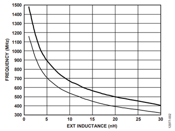
Figure 2. Output center frequency vs. external inductance.
The relatively wide 100 MHz tuning range is made possible by the use of eight tuning bands, as shown in Figure 3. Similar to the inductor selection, ADIsimPLL selects the tuning band that is approximately centered, Band 4 or Band 5 (as counted from the left), and with a tuning voltage of 1.875 V. This horizontal and vertical centering provides the calibration engine with the greatest flexibility.

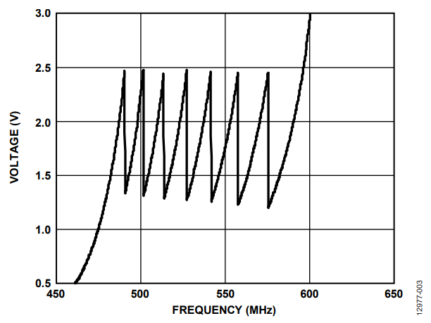
Figure 3. Frequency vs. VTUNE.
Within any one band, VTUNE must be limited to the range from 1.25 V to 2.5 V to maintain optimum performance. It is possible to exceed these limits; however, exceeding the limits can produce an incorrect output frequency and/or poor spurious performance.
Calibration Process
When the device performs a frequency calibration, it determines which VCO band is the optimal band for the desired output frequency. This is followed by the adjustment of VTUNE in normal closed-loop PLL operation to lock to the correct frequency.
During the calibration process, the divided down VCO frequency (fVCO/((PB + A) × BSC)) is compared to the divided down PFD reference frequency (fPFD/BSC). Because the prescaler is clocked by the VCO and does not have a synchronous reset, there is always an uncertainty of P × VCO cycles in the divided down VCO frequency.
Figure 4 shows this uncertainty error for a prescaler value of 8 as the N word (PB + A) is varied with all BSC divider settings.

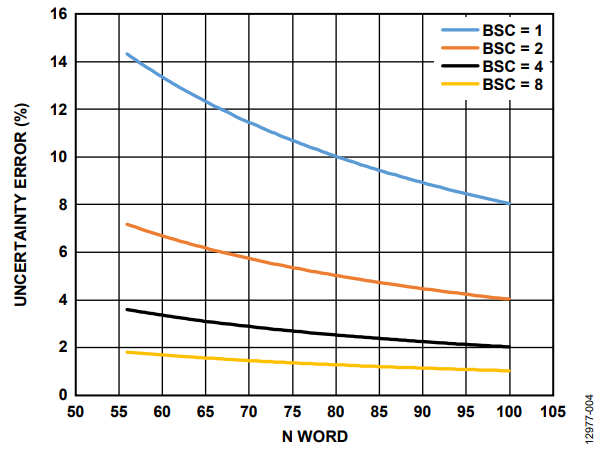
Figure 4. Uncertainty error vs. N word.
The uncertainty error manifests itself as an error in the output frequency. A design example is carried through this application note to explain the uncertainty error.
When operating with low RF frequencies, use the maximum BSC value and minimum PFD frequency possible so that this percentage uncertainty error is minimized.
For example, if the VCO frequency is 400 MHz and P = 8, the output of the prescaler is 50 MHz; therefore, there is an uncertainty of 1/50 MHz = 20 ns between POUT driving the calibration circuit and the next rising edge of the N counter output, which goes to the PFD.
It takes five clock periods for the successive approximating circuit to select the proper band. The calibration clock period is defined in the following equation. BSC can be programmed for values of 1, 2, 4, or 8.
Calibration Clock Period = (1/RCLOCK) × BSC
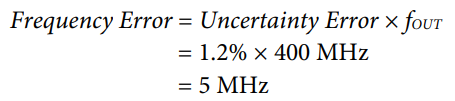
Continuing with the previous example, with R clock = 5 MHz and BSC = 8, the calibration time is 1.6 µs. Assuming the same 20 ns uncertainty derived previously, the uncertainty error is calculated as follows:
Uncertainty Error = (20 ns/1.6 µs) × 100% = 1.25%
At a 400 MHz desired output frequency, the uncertainty error causes a frequency error of:
Taking the example one step further, see Figure 5. For the 400 MHz output, ADIsimPLL indicates that an inductor value of 24 nH is needed. For this inductance, the VCO sensitivity, KV, is approximately 7.5 MHz/V.

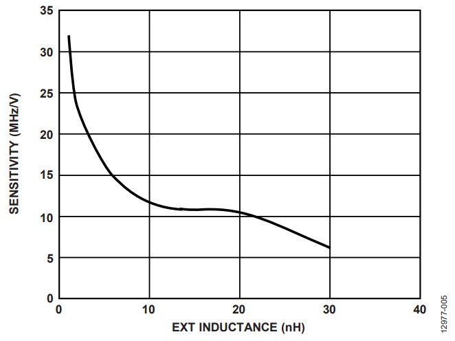
Figure 5. Tuning sensitivity vs. inductance.
Dividing the frequency error by KV gives the magnitude of the VTUNE error voltage.
VTUNE Error = 5 MHz ÷ 7.5 MHz/V = 0.67 V
The VTUNE error voltage can drive the desired VTUNE voltage beyond the specified limits of 1.25 V to 2.5 V. Figure 6 shows this VTUNE error voltage vs. RF frequency and PFD frequency.

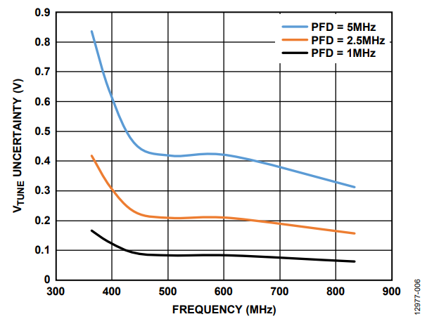
Figure 6. VTUNE error.
Figure 7 shows how one frequency band overlaps the adjacent band. A 24 nH inductor generates an output frequency of 400 MHz. In an ideal design, this is the L1 inductor, shown in Figure 7. As VTUNE is adjusted to fine tune the output frequency, VTUNE moves up or down the curve while staying within the same band and within the limits of 1.25 V to 2.5 V.


Figure 7. VTUNE tuning curve.
Component tolerances can cause the output frequency to be not centered. The calibration engine attempts to adjust the VTUNE voltage to compensate; however, this can be made more difficult because of the VTUNE error voltage. The real inductor may place the frequency at the point labeled L2 (see Figure 7). L2 is in Band 5 but near the lower limit of 1.25 V. With the uncertainty error in the calibration circuit, the calibration circuit may try to select Band 4, which requires VTUNE to exceed the 2.5 V limit. If VTUNE gets close to the VDD rail, the charge pump degrades, which negatively impacts the output frequency performance.
This demonstrates that the input REFIN, fOUT, and the R, N, and BSC counter values must all be considered to ensure that the ADF4360-7 VTUNE voltage stays within the range of 1.25 V to 2.5 V.
Avoiding VTUNE Problems
The performance specifications in the ADF4360-7 data sheet are based on operating within the specified VTUNE range of 1.25 V to 2.5 V. The calibration circuit operates when VTUNE is between 1.0 V and 0.6 V below VDD; outside of this range, performance may be degraded because the charge pump is out of its compliance range, which results in an increase in spurious and phase noise. Using these values, it is possible to determine limits for the R and N counter values as a function of REFIN, KV, RCOUNT, P, and BSC.
As shown previously, there is an uncertainty error due to nonsynchronous clocking between the POUT and the A and B counters. The uncertainty can be calculated as follows:

where:
P is the prescaler value.
REFIN is the input reference frequency.
RCOUNT is the R counter.
BSC is the band select divider.
KV is the PLL sensitivity.
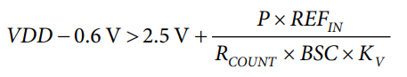
The desired VTUNE operating range is 1.25 V to 2.5 V. However, the device operates, with some degradation, when VTUNE is between 1.0 V and VDD − 0.6 V. Starting with the lower limit, when the VTUNE error voltage is subtracted from the lower VTUNE limit, the difference should be greater than 1 V. This difference can be expressed as follows:

Rearranging and solving for RCOUNT determines the minimum R value that ensures the lower limit of VTUNE stays within its operating range.
From the previous example, P = 8, REFIN = 10 MHz, BSC = 8, and KV = 7.5 MHz/V. Plugging these numbers into the equation results in RCOUNT ≥ 6.
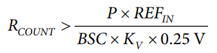
The minimum R value that ensures the upper VTUNE limit is not exceed must also be evaluated. In this case, the sum of VTUNE and the VTUNE error voltage should be less than VDD − 0.6 V. This sum can be expressed as follows:
Solving for RCOUNT results in the following equation:
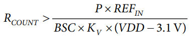
Using the same values for BSC, KV, P, and REFIN and setting VDD to 3.3 V results in RCOUNT ≥ 7. To ensure VTUNE compliance, use the larger of the two RCOUNT values (7 in this case).
The N value is then calculated using the following equation:
NCOUNTER = VCOOUT × RCOUNT/REFIN
The R and N counter values must be selected so that they fall within the limits for these values, as specified in the ADF4360-7 data sheet.
For the design example, it was determined that the R counter value must be greater than or equal to 7. The least common multiples for the desired 400 MHz output indicate that one option is to set the R counter equal to 10 and the N counter to 400 (P = 8, A = 0, and B = 50), which results in a PFD frequency of 1 MHz. This is the same solution produced by ADIsimPLL.
Sumarry
Begin by simulating the design using ADIsimPLL. If the simulation produces an acceptable design, no further work is required. Verify the simulation by testing the circuit using an Analog Devices evaluation board. If changes are needed to the ADIsimPLL design, the following are suggestions to minimize the uncertainty error and to maximize the design margin.
- For the best phase noise performance, set the R counter value as small as possible but large enough to keep the VTUNE error voltage within limits.
- Using the largest value for BSC provides the maximum calibration time and reduces the uncertainty error.
- Use the smallest prescaler value possible to reduce the uncertainty error.
- Use the largest possible voltage for VDD to provide the widest margin of VTUNE error voltage.
- If either calculation for determining the minimum value of RCOUNT results in a negative number, no solution will ensure that VTUNE stays within an acceptable operating range.
- A least common multiple (LCM) program can be helpful for finding integer values for N and R counter values.
Author
