AN-1333: Architecting a Direct, 3-Phase Energy Meter with Shunts Using the ADE7932/ADE7933/ADE7978
Introduction
The ADE7932/ADE7933/ADE7978 isolated metering chipset targets the polyphase energy metering applications using shunt current sensors. This application note expands on the Applications Information section of the ADE7932/ADE7933/ADE7978 data sheet. It provides in-depth explanations of how to use the chipset when developing a direct, 3-phase meter with shunts.
Architecting A Direct, 3-Phase Meter Using The ADE7932/ADE7933/ADE7978
Figure 1 shows how a direct, 3-phase energy meter using the ADE7932/ADE7933/ADE7978 isolated metering chipset is connected in a 3-phase, 4-wire system. Phase A connects to Terminal 1 and Terminal 3 of the meter, Phase B connects to Terminal 4 and Terminal 6 of the meter, Phase C connects to Terminal 7 and Terminal 9 of the meter, and the neutral line connects to Terminal 10 and Terminal 12 of the meter.


Figure 1. 3-phase, 4-wire, direct meter connections.
Figure 2 presents how a meter that uses the chipset is architected. Three shunts are connected to the meter terminals where the 3-phase, 4-wire connections are made. Every ADE7932/ADE7933 device manages one phase through some interface circuitry. The reference terminal of the shunt becomes the ground of the isolated side of the ADE7932/ADE7933. The GND_A reference terminal is the ground of the Phase A ADE7932/ADE7933 isolated side, the GND_B reference terminal is the ground of the Phase B ADE7932/ADE7933 isolated side, and the GND_C reference terminal is the ground of the Phase C ADE7932/ADE7933 isolated side. The resistor dividers, R1_x and R2_x, where x = A, B, and C, sense the voltage between the A, B, and C phase lines and the neutral line. The current channel analog-to-digital converter (ADC) of every ADE7932/ADE7933 measures the voltages across the shunts, while the V1 voltage channel ADC measures the voltages across the R1_x resistors.


Figure 2. Shunt-based, direct, 3-phase meter architecture.
The ADE7978 manages the ADE7932/ADE7933 through a bit stream interface. The microcontroller (MCU) manages the ADE7978 using either the serial port interface (SPI) or I2C communication. If I2C communication is used, the MCU can also use the high speed data capture (HSDC) port for meters that must analyze the currents and voltages beyond what the ADE7978 offers. The HSDC port is a master SPI port that the ADE7978 uses to send out various instantaneous metering quantities.
Note that the typical voltage terminals, Terminal 2, Terminal 5, and Terminal 8, of the meter are not used when the meter is based on the chipset. The reference terminals of the shunts (GND_A, GND_B, and GND_C) that are directly connected to the phase lines become the reference points for the voltage sensing resistor dividers.
The interface circuitry between the shunts, the voltage dividers, and the ADE7932/ADE7933 devices is discussed in the Interfacing the ADE7932/ADE7933 with the Shunt and the Resistor Divider section.
The neutral line determines the ground of the microcontroller (GND_MCU) that manages the chipset, which is the same ground of the ADE7978 and of the primary side of the ADE7932/ADE7933. The MCU uses the SPI or the I2C interface to communicate with the ADE7978, which also means that the power supply of the meter must provide a supply voltage to the microcontroller and to the chipset that has GND_MCU on the neutral line.
For the meter presented in Figure 2, the neutral line current is not monitored. Figure 3 presents the architecture of a direct, 3-phase meter in which the neutral current is monitored. The only difference is an additional ADE7932 (Phase N) that senses only the neutral line current using a shunt. The voltage channel of this chip is not used.

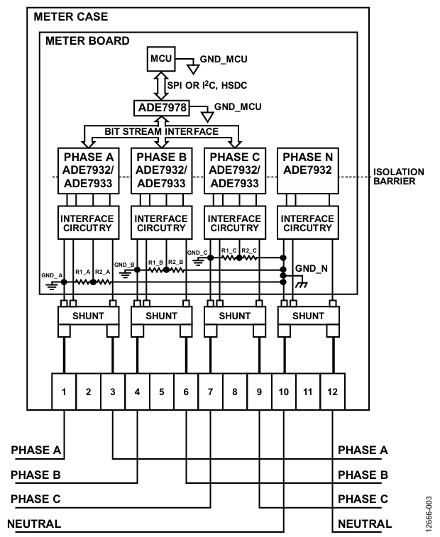
Figure 3. Figure 3. Shunt-based, direct, 3-phase meter architecture with monitored neutral line.
The MCU, the ADE7978, and the primary side of the ADE7932/ADE7933 have a GND_MCU isolated ground from the neutral line. This architecture means the power supply of the meter must provide a supply voltage to the MCU and to the chipset that is isolated from the neutral line.
Interfacing The ADE7932/ADE7933 With The Shunt And The Resistor Divider
All of the ADE7932/ADE7933 devices that monitor the phase lines have the same interface circuitry. The interface circuitry is composed of two paths: one that interfaces the ADE7932/ADE7933 with the shunt (see Figure 4) and one that interfaces the ADE7932/ ADE7933 with the voltage divider (see Figure 5).


Figure 4. Interfacing the ADE7932/ADE7933 with a shunt.

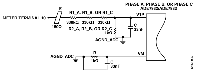
Figure 5. Interfacing the ADE7932/ADE7933 with a voltage divider.
A shunt senses the Phase A, Phase B, Phase C, or Phase N current (see Figure 4). The antialiasing filter, R/C (1 kΩ/33 nF), between the IP pin and the IM pin, and the shunt terminals have a corner at 4.8 kHz (1/(2 × π × 103 × 33 × 10-9)). The AGND_ADC ground point where the filter capacitors are biased is connected to the GND_A reference terminal, the GND_B reference terminal, the GND_C reference terminal, or the GND_N reference terminal of the shunts.
The Phase A, Phase B, or Phase C to neutral voltages are sensed by the voltage dividers, R1_x and R2_x, where x = A, B, or C (see Figure 5). Resistor R1_x is composed of three 330 kΩ resistors and R2_x is 1 kΩ. This resistor divider ensures a full-scale voltage equal to the following:

This full-scale voltage is sufficient to monitor 230 V, 3-phase systems. The capacitor, C (33 nF), parallel to R2_x, creates the antialiasing filter in the V1P pin path. Between the ground point, AGND_ADC, derived from the ground terminal, GND_x, of the shunt (see Figure 4), and the VM pin of the ADE7932/ADE7933 (see Figure 5), there is an identical antialiasing filter, R/C (1 kΩ/33 nF). Note that the antialiasing filters in both current paths and voltage paths are the same, which ensures that the delays introduced in the phase current and voltage measurements are similar.
The E ferrite beads (150 Ω at 100 MHz) are placed in the shunt and voltage divider connections to filter the high frequency noise that may be induced into the wires during electrical fast transient (EFT) tests.
As the meter architectures considered in Figure 2 and Figure 3 do not present any additional voltages to measure besides the phase to neutral voltages, Figure 5 does not present the circuitry required to interface the V2P pin of the ADE7933. However, if additional voltages must be monitored, the V2P pin circuitry is identical to the V1P pin circuitry. The V2P pin functionality is available only on the ADE7933. The V2P pin functionality is not available on the ADE7932.
Providing Clock Signal To ADE7978
See the ADE7932/ADE7933/ADE7978 data sheet for details on providing a clock to the ADE7978.
Communicating With The ADE7978
The ADE7978 has an SPI interface multiplexed with an I2C interface. The ADE7932/ADE7933/ADE7978 data sheet provides extensive details on the protocol used to read to and write from the device registers.
In the following, a system perspective of the MCU managing the ADE7978 in a 3-phase energy meter is proposed. Both I2C and SPI communications are analyzed. I2C functions at the maximum serial clock frequency of 400 kHz, while the SPI functions at the maximum serial clock frequency of 2.5 MHz.
The ADE7978 has 90 configuration registers: 63 that are sent to the ADE7978 in 32-bit format, 15 registers that are 16 bits wide, and 12 registers that are 8 bits wide.
At maximum serial clock frequency, the time it takes to write all 90 configuration registers into the ADE7978 at power up or after a reset is different for I2C and SPI usage.
If I2C is used, it is:

If SPI is used, it is:

The configuration registers must be read back to ensure that they have been captured correctly by the ADE7978. At maximum serial clock frequency, the time to read back all 90 registers is different for I2C and SPI usage.
If I2C is used, it is:
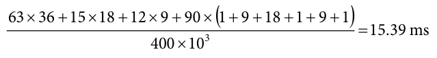
If SPI is used, it is:

Note that these timings do not consider the inefficiencies of the MCU in servicing the I2C and SPI ports without any delay. These are the shortest timings users can achieve when writing and reading all the configuration registers of the ADE7978.
The ADE7978 provides data out at a frequency of 8 kHz. Many output registers, such as the energy registers (the AWATTHR register, for example), do not need to be read so frequently.
If I2C is used, the HSDC port is available. Enable the HSDC port to get the instantaneous values of various phase voltages, currents, and powers if advanced metrology functionality, not provided by the ADE7978, is required.
If SPI is used, the HSDC port is not available. Use the SPI burst read functionality to access all the instantaneous phase voltages and currents contained from Address 0xE50C to Address 0xE512. The time to read them is:

This timing is the minimum access time possible because the programming inefficiencies of the MCU raise it. Because these registers are updated every 8 kHz, the margin to accommodate them is:

Layout Guidelines
Figure 6 presents the schematic of the metrology section of a direct, 3-phase meter using four ADE7933 devices. It is the schematic of the ADE7978 evaluation board. The second voltage channel, V2P, is shown with a voltage divider to provide the most comprehensive layout example possible.


Figure 6. Direct, 3-phase meter schematic of metrology section.
A 4-layer printed circuit board (PCB) is required when using the chipset. The devices pass Class B CISPR22/EN-55022 standard specification with a sufficient margin only with a 4-layer PCB (see the Radiated Emission Tests Results section for details on these results). The top and bottom layers are identical to a 2-layer PCB design, and the inner layers create a stitching capacitor. The presence of the stitching capacitor is essential to reducing the emissions generated by the ADE7932/ADE7933 dc-to-dc converters and meet the standard requirements.
Figure 7 presents the structure of the 4-layer PCB. The top layer contains the components. Layer 2 creates one plate of the stitching capacitor using the GNDISO isolated ground plane of the ADE7932/ADE7933. Layer 3 creates the other plate of the stitching capacitor using the GND_MCU primary ground plane of the ADE7932/ADE7933 devices. Note that the PCB thickness between the plates is 0.5 mm. The standard IEC 62052-31 requires a minimum thickness of 0.4 mm when the lines to neutral voltages are below 300 V, but a 0.5 mm thickness allows any PCB production variation.


Figure 7. 4-layer structure with stitching capacitor.
Do not invert Layer 2 with Layer 3 (that is, set the GND_MCU plane on Layer 2 and the GNDISO plane on Layer 3) because the GND_MCU plane creates a parasitic capacitance with the shunt related PCB traces on the top layer. This parasitic capacitance creates a voltage that adds to the voltage across the shunt and is proportional and in phase with the voltage between the GNDISO plane and the GND_MCU plane. The added voltage affects the accuracy of the metrology measurements. By setting the GNDISO plane on Layer 2 and the GND_MCU plane on Layer 3, the GNDISO planes shield the GND_MCU plane and remove the coupling to the PCB traces of the IP pin and the IM pin of the shunt on the top layer.
Figure 8, Figure 9, Figure 10, and Figure 11 present the recommended 4-layer layout of the Figure 6 metrology section. It is the layout implemented in the ADE7978 evaluation board.


Figure 8. Top layer layout of the direct, 3-phase meter metrology section.


Figure 9. Layer 2 layout of the direct, 3-phase meter metrology section.


Figure 10. Layer 3 layout of the direct, 3-phase meter metrology section.


Figure 11. Bottom layer layout of the direct, 3-phase meter metrology section.
ADE7932/ADE7933 Decoupling Capacitors Layout Guidelines
Follow these recommendations for the decoupling capacitors between the VDD pin and the GND pin (10 µF and 100 nF), the VDDISO pin and the GNDISO pin (10 µF and 100 nF), the LDO pin and the GNDISO pin (4.7 µF and 100 nF), and between the REF pin and the GNDISO pin (4.7 µF and 100 nF) of the ADE7932/ADE7933:
- Place the 100 nF capacitors closest to the chip.
- Make the connections between the capacitors and the VDD pin, the VDDISO pin, the LDO pin, and the REF pin as short as possible.
- Make the connections between the capacitors and the GND pin, the GNDISO pin, the LDO pin, and the REF pin as short as possible.
This setup improves the electromagnetic compatibility (EMC) immunity of the chips and lowers the emissions generated by the ADE7932/ADE7933 dc-to-dc converters.
Figure 12, Figure 13, Figure 14, and Figure 15 present the various layouts of these capacitors.


Figure 12. Layout of capacitors between the VDD pin and the GND pin.


Figure 13. Layout of capacitors between the VDDISO pin and the GNDISO pin.


Figure 14. Layout of capacitors between the LDO pin and the GNDISO pin.


Figure 15. Layout of capacitors between the REF pin and the GNDISO pin.
ADE7932/ADE7933 Isolated Ground Layout Guidelines
The ADE7932/ADE7933 have two GNDISO isolated ground pins. The GNDISO pins are connected through ferrites to the reference terminal of the shunt and determine the isolated ground plane on the top layer of the PCB. The connections between the GNDISO pins and the isolated ground plane must be very short. To have the lowest inductance possible, the vias that connect the isolated ground plane from the top layer to the stitching capacitor plate on Layer 2 must be close to the GNDISO pins (see Figure 16). Limit the number of vias to the minimum because they take area from the stitching capacitor plates and therefore reduce its capacitance.


Figure 16. Layout of GNDISO connections to isolated ground plane and related vias.
Plates on Layer 2 and Layer 3 create the stitching capacitor. Figure 17 shows the layout of one plate created underneath Phase A of the ADE7932/ADE7933. The vias that are circled in red connect the Layer 2 plate to the GNDISO plane from the top layer. Figure 18 shows the layout of the GND_MCU plane in Layer 3. This plane creates the plate of four stitching capacitors, one for each ADE7932/ ADE7933. The vias circled in red are the GNDISO vias. More than 1 mm of space is between these vias and the GND_MCU plate, which complies with the IEC 62052-31 standard that requires 0.4 mm minimum distance between adjacent conductors when the line to neutral voltages are below 300 V.


Figure 17. Section of layer 2, creating stitching capacitor GNDISO plate.


Figure 18. Section of layer 3, creating stitching capacitor GNDMCU plate.
The minimum stitching capacitor area that is recommended to pass Class B CISPR22/EN-55022 standard specification is 825 mm2, giving a capacitor value of 63 pF (see the Radiated Emission Tests Results section for more details).

where:
ε0 is the vacuum permittivity and equals 8.854 × 10⁻¹² F/m.
εr is the relative permittivity of the PCB FR4 material and equals 4.3.
A is the area of the capacitor plates and equals 825 mm2.
d is the distance between the plates and equals 0.5 mm.
Increasing the area of the plates leads to a larger capacitor value, which yields a bigger margin in passing the Class B CISPR22/EN-55022 standard. In the ADE7978 evaluation board, there is 7.62 mm of space between the GNDISO plates of various ADE7933 devices on Layer 2, even though the IEC 62052-31 standard requires 0.4 mm minimum distance between adjacent conductors when the line to neutral voltages are below 300 V (see Figure 19). The capacitor value is 84 pF for an area of the plates equal to 1100 mm2.


Figure 19. Section of layer 2 showing all four stitching capacitors.
ADE7978 Placement on Board Guidelines
Place the ADE7978 symmetrically relative to Phase A and Phase C of the ADE7932/ADE7933 devices and close to Phase B of the ADE7932/ADE7933 (see Figure 20). Phase N of the ADE7933 can be placed somewhat farther from the ADE7978 because Phase A, Phase B, and Phase C of the ADE7932/ADE7933 devices provide data upon which the meter executes the billing, and the integrity of these signals must be as high as possible. Shield the traces of the connections between the ADE7978 and the ADE7932/ADE7933 devices. Ensure that the GND_MCU ground plane around ADE7978 is solid to avoid corruption of the bit stream communication during EMC tests.


Figure 20. ADE7978 placed symmetrically to phase A and phase C of the ADE7933 and close to phase B of the ADE7933.
ADE7978 Crystal and Load Capacitors Layout Guidelines
Place the load capacitors of the crystal closest to the ADE7978 to improve the EMC immunity of the chip, whereas the crystal can be placed in close proximity (see Figure 21). The distance between the crystal and the load capacitors is not as critical as the distance between the capacitors and the XTALIN pin and the XTALOUT pin.


Figure 21. Layout of the ADE7978 crystal.
ADE7978 Decoupling Capacitors Layout Guidelines
Follow these recommendations for the decoupling capacitors between the VDD pin and the GND pin of the ADE7978 (10 µF and 100 nF), and between the LDO pin and the DGND pin (4.7 µF and 100 nF):
- Place the 100 nF capacitors closest to the chip.
- Connect the capacitors to the VDD pin and the LDO pin with traces as short as possible.
- Connect the capacitors to the GND pin and the DGND pin with traces as short as possible.
- Make a solid ground plane (GND_MCU of the meter) around the ADE7978.
This setup improves the EMC immunity of the ADE7978 (see Figure 22).


Figure 22. Layout of the ADE7978 decoupling capacitors and exposed pad.
ADE7978 Exposed Pad Guidelines
The ADE7978 package has a 3.3 mm × 3.3 mm exposed pad underneath the package. Create a similar pad on the PCB under the exposed pad and solder the exposed pad to it to confer mechanical strength to the package. Then, connect the pads to the GND pin and the DGND pin, as shown in Figure 22.
Radiated Emission Tests Results
The ADE7978 evaluation board was tested for compliance with the Class B CISPR22/EN-55022 standard. The board was placed in a 3-phase meter case and was powered from a battery. A 5 m, 3-phase cable, without termination, was mounted on the meter and then placed under the floor in the anechoic chamber. Note that the ADE7978 evaluation board contains four ADE7933 isolated ADCs.
Measurements of the radiated emissions were executed for frequencies between 30 MHz and 1 GHz and between 1 GHz and 2 GHz.
With a stitching capacitor of 84 pF (1,100 mm2 plates), a minimum 11 dBµV/m quasi peak margin to Class B CISPR22/EN-55022 limits was obtained for frequencies between 30 MHz and 1 GHz (see Figure 23). For frequencies between 1 GHz and 2 GHz, a minimum 10 dBµV/m average results margin to Class B CISPR22/EN-55022 limits was obtained (see Figure 24).


Figure 23. Anechoic chamber emissions from ADE7978 evaluation board, 84 pF ftitching capacitor (quasi peak points in blue, 30 MHz to 1 GHz).


Figure 24. Anechoic chamber emissions from ADE7978 evaluation board, 84 pF stitching capacitor (average points in green, 1 GHz to 2 GHz).
An ADE7978 evaluation board with a stitching capacitor of 63 pF (825 mm2) was used to test the radiated emissions when the stitching capacitor is smaller than 84 pF. The ADE7978 evaluation board passed Class B CISPR22/EN-55022 specification by a 9 dBµV/m quasi peak margin for frequencies between 30 MHz and 1 GHz (see Figure 25) and a 7 dBµV/m average results margin for frequencies between 1 GHz and 2 GHz (see Figure 26).


25. Anechoic chamber emissions from ADE7978 evaluation board, 63 pF stitching capacitor (quasi peak points in blue, 30 MHz to 1 GHz).


Figure 26. Anechoic chamber emissions from ADE7978 evaluation board, 63 pF stitching capacitor (average points in green, 1 GHz to 2 GHz).
PCB designs that have stitching capacitors smaller than 63 pF (that is, with the area of the plates smaller than 825 mm2) are not recommended. For example, with a stitching capacitor of 42 pF (an area of the plates of 550 mm2), an ADE7978 evaluation board was over the Class B CISPR22/EN-55022 limit by 4 dBµV/m at 380 MHz.
Conclusions
This application note has shown how to develop a direct, 3-phase meter with shunts using the ADE7932/ADE7933/ADE7978 isolated metering chipset. It provided recommendations on the schematic and layout to pass the Class B CISPR22/EN-55022 radiated emissions specification by a margin of at least 10 dBµV/m. It showed how much bandwidth an MCU has to reserve for managing the I2C, SPI, or HSDC communications with the ADE7978.
Authors
