AN-1320: ADuCM360/ADuCM361 Self Diagnostic Features
Introduction
The ADuCM360/ADuCM361 are 32-bit, Cortex™-M3-based microcontrollers that also integrate 24-bit ∑-Δ analog-to-digital converters (ADC), each with a fully programmable instrumentation amplifier on the front end. These microcontrollers target a wide range of applications including industrial control and instrumentation applications. In many of the target applications, self diagnostic features are important in safety critical environments and smart recovery from failure modes.
This application note describes some of the ADuCM360/ADuCM361 features that diagnose issues with the ADuCM360/ADuCM361 and surrounding circuitry.
Diagnostic Current Sources
The ADuCM360/ADuCM361 contain two 50 µA diagnostic current sources. These current sources are different from the programmable excitation current sources. ADC0 and ADC1 have separate, independent diagnostic current sources.
The diagnostic current sources are routed internally to the analog input channels currently selected for ADC conversions via the positive input channel selection, the ADCxCON register, Bits[9:5], and the negative input channel selection, the ADCxCON register, Bits[4:0]. As shown in Table 1, the ADCxCON register, Bits[11:10], enable/disable current sources to the positive and negative ADC inputs.
| Bits | Bit Name | Description |
| [11:10] | ADCDIAG | Diagnostic current bits. 00: Current source off. 01: Enable a 50 µA current on the selected positive input. For example, AIN0. 10: Enable a 50 µA current on the selected negative input. For example, AIN1. 11: Enable a 50 µA current on the selected input. For example, AIN0 and AIN1. |
| Diagnostic Test | Normal Result | Fault Result | Detected Measurement for Fault | |||
| Register ADCxCON, Bits[11:10], Setting | Current Source Description | Description | ||||
| 00 | Current source off | Convert on AINx and AINy as normal with diagnostic currents disabled | Normal Result | Not Applicable | Not Applicable | |
| 01 | Enable a 50 µA diagnostic current source on AINx | Convert AINx and AINy | ADC changes by ΔV = 50 µA × R1; for example, ~100 mV for R1 = 2 kΩ | Short circuit between AINx and AINy; short circuit between R1_A and R1_B | ADC reading ≈ 0 V, regardless of programmable gain amplifier (PGA) setting | |
| 01 | Enable a 50 µA diagnostic current source on AINx | Convert AINx in single-ended mode | Expected voltage on AINx | AINx open circuit or R1 open circuit | ADC reading is positive full scale, even on the lowest PGA setting | |
| 11 | Enable a 50 µA diagnostic current source on both AINx and AINy | Convert AINx and AINy | ADC reading hanges by ΔV = 50 µA × (R1 − R2), that is, ~10 mV for 10% tolerance | R1 does not match R2 | ADC reading > 10 mV of expected value | |
| 1 AINx is the positive input channel and AINy is the negative input channel. | ||||||
For example, if the ADCxCON register, Bit 11 = 0x1 and the ADCxCON register, Bits[4:0] = 0x1, a 50 µA current flows from AIN1.
Similarly, if the ADCxCON register, Bit 10 = 0x1 and the ADCxCON register, Bits[9:5] = 0x0, a 50 µA current flows from AIN0.
Figure 1 shows an example circuit.
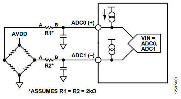
Figure 1. Example Circuit Using Diagnostic Current Sources.
Fully Flexible Analog Input Mux
The ADuCM360/ADuCM361 ADCs have a fully flexible analog input mux. Because of the fully flexible analog input mux, the user is not constrained with fixed differential input pairs for ADC measurements. It is possible to configure a differential pair with any external analog input pins. In addition, ADC1 allows any external analog input pin to be paired with one of the internal ADC channels for a differential ADC1 measurement. Both ADC0 and ADC1 can be connected to any external analog input pin.
The fully flexible analog input mux is useful for checking the following system failures:
- Analog input pin voltage check. Cross check vs. a known supply voltage, vs. a VDAC voltage, or relative to a fixed external voltage connected to one of the AINx pins.
- Functional check on either of the ADCs (ADuCM360 only). Repeat measurement taken on ADC0 by selecting same input channels and repeating on ADC1. It is also possible to check the ADC1 reading via ADC0.
- Monitor the digital or analog supply voltages via ADC1. This is useful for battery-powered applications or for detecting a decaying power supply.
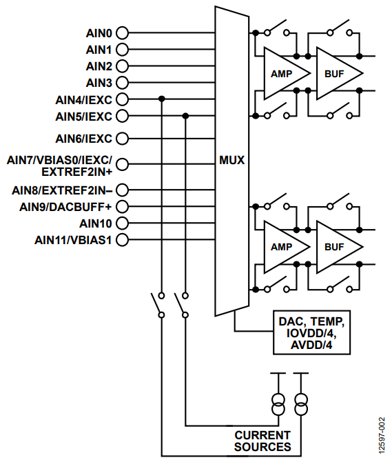
Figure 2. ADC Input Mux.
Multiple ADC Reference Sources
Table 3 shows the reference options available for ADC0 and ADC1. The reference options are selected via the ADCxCON register, Bits[13:12].
| Bits | Bit Name | Description |
| [13:12] | ADCREF | Reference selection. 00: INTREF-AGND. 01: EXTREF. The external buffer mode is set in the ADCxCFG register. 10: EXTREF2IN (valid for ADC1 only). EXTREF2IN+ buffer controlled via the ADCxCFG register. 11: AVDD-AGND. |
Reference options allow safety checking of an external reference source by repeating the measurement using the internal reference or by using the analog supply voltage as the ADC reference source.
This safety checking allows ADuCM360/ADuCM361 systems to detect a failure with any of the ADC voltage reference sources.
Another feature for the external reference, EXTREF, is the detection of a drop in the reference voltage that sets a register status bit. For EXTREF, the status bit in the DETSTA register, Bit 4, is set to 1 if the source voltage of EXTREF across VREF+ and VREF− drops below 0.4 V (typical) or below 0.8 V (maximum). To use this feature, set the DETCON register, Bit 8, to 1.
This feature does not work for the EXTREF2IN± reference source.
Verification of Flash Contents
Along with read/write flash protection mechanisms, the ADuCM360/ADuCM361 also support a function to verify the contents of user flash that have not changed since last programmed; this is the sign feature. More details regarding this feature are available in the UG-367 User Guide.
Flash Integrity Signature Feature
The signature checks the integrity of the flash device. The software can call a signature check command occasionally or whenever a new block of code is about to be executed. The signature is a 24-bit cyclic redundancy check (CRC) with the polynomial x24 + x23 + x6 + x5 + x + 1.
The sign command generates a signature and checks the signature of a block of code, where a block can be a single page or multiple pages. A 24-bit linear feedback shift register (LFSR) generates the signature. The hardware assumes that the signature for a block is stored in the upper four bytes of the most significant page of a block. These four bytes are not included when generating the signature.
Use the following procedure to generate a signature:
- Write the start address of the block to the FEEADR0L register and the FEEADR0H register
- Write the end address of the block to the FEEADR1L register and the FEEADR1H register.
- Write the sign command to the command register (the FEECMD register = 10).
When the command completes, the signature is available in the sign register. The signature is compared with the data stored in the upper four bytes of the uppermost page of the block. If the data does not match the signature, a fail status is returned in the status register (the FEESTA register, Bits[5:4] = 10).
While the signature is being computed, all other accesses to flash are stalled for a 128 kB block, that is, 32,000 reads.
Note that the FEEADR0L register, the FEEADR0H register, the FEEADR1L register, and the FEEADR1H register are byte addresses, but only pages must be identified. The hardware ignores the lower nine bits.
Note that the user must run the CRC polynomial in user code first to generate the CRC value and must then write this to the upper four bytes of the uppermost page of a block. When this operation is complete, any call of the signature feature compares this 4-byte value to the result of the signature check function.
Integrity of the Kernel
The hardware automatically checks the integrity of the kernel after reset. In the event of a failure, the FEESTA register, Bit 6, is set and user code cannot run. This bit can be read via a serial wire read only if the serial wire interface is enabled.
ESD Protection On All External Pins
Each external pin on the ADuCM360/ADuCM361 has a protection circuit to ground and to the supply rail to protect the device from electrostatic discharges due to operator or machine handling.
Table 4 shows details about the robustness of the device to transients from the ADuCM360/ADuCM361 reliability reports.
| ESD Model | Package | ESD Test Specification | RC Network | Highest Pass Level | First Fail Level | Class |
| FICDM | 48-lead LFCSP | JESD22-C101 | R = 1 Ω, C = capacitance of the package | ±1500 V | Not applicable | C6 |
| HBM | 48-lead LFCSP | ESDA/JEDEC JS-0012011 | R = 1.5 kΩ, C = 100 pF | ±2500 V | ±3000 V | 2 |
Cortext-M3 Fault Management Features
The fault management system of the Cortex-M3 processor detects bus, memory, and undefined instruction faults.
When these occur, the Cortex-M3 processor stops executing its current instruction and vectors to a fixed memory address where an associated user defined exception handler is executed.
In this exception handler function, the user code can alert the system of the fault and proceed with next steps to recover from the failure or else shut down the ADuCM360/ADuCM361.
Table 5 summarizes the key exceptions.
| Number | Type | Prioriity | Description |
| 1 | Reset | -3 (highest) | Any reset |
| 2 | NMI | -2 | Nonmaskable interrupt connected to power supply monitor of ADuCM360/ADuCM361 |
| 3 | Hard fault | -1 | All fault conditions if the corresponding fault handler is not enabled |
| 4 | Memory management fault | Programmable | Memory management fault; access to illegal locations |
| 5 | Bus fault | Programmable | Prefetch fault, memory access fault, data abort, and other address/memory related faults |
| 6 | Usage fault | Programmable | Same as undefined instruction executed or illegal state transition attempt |
Clock and Timers
The ADuCM360/ADuCM361 integrate two on-chip oscillators and circuitry for an external crystal as follows:
- LFOSC is a 32 kHz low power internal oscillator, used in low power modes.
- HFOSC is a 16 MHz internal oscillator that is used in active mode.
- LFXTAL is a 32 kHz external crystal.
- Power saving clock mechanism, which can be enabled and disabled for a peripheral.
Clocking Architecture Block Diagram
Using software control, a user may select from a choice of four different system clock sources to allow cross checking of other clock sources and internal clock circuits.
Note that, by default, the internal 16 MHz oscillator is the system clock (UCLK) source.
The ADuCM360/ADuCM361 also integrate a watchdog timer. The watchdog timer is normally enabled in user code to be refreshed regularly. If user firmware does not run as expected and fails to refresh the watchdog timer within a predefined period, the watchdog hardware issues a full system reset.
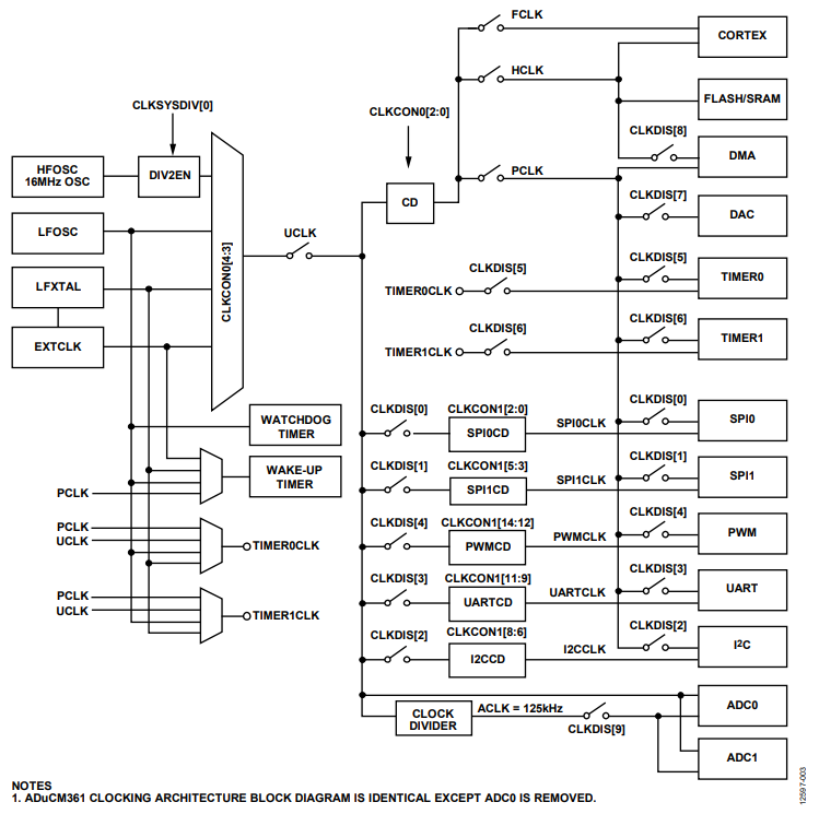
Figure 3. ADuCM360 Clocking Architecture Block Diagram.