AN-1269: Designing an Inverting Power Supply Using the ADP2441/ADP2442 Synchronous Step-Down DC-to-DC Regulators
Introduction
Applications such as bipolar amplifiers, optical modules, CCD bias, and OLED displays usually require a negative output voltage from a positive input voltage. Designers of power management systems need versatile switching controllers and regulators that allow them to solve these power management challenges. The ADP2441/ADP2442 switching regulators from Analog Devices, Inc., provide synchronous buck functionality. This ranges from a 36 V input voltage down to 0.6 V output voltage at up to 1 A with a switching frequency range from 300 kHz to 1 MHz.
Although targeted for synchronous step-down applications, the versatility of the ADP2441/ADP2442 allows these parts to realize an inverting buck boost topology, which can generate a negative output voltage from a positive input voltage, without additional cost, component count, or solution size.
These parts utilize synchronous topology, which gives higher efficiency at a full load and lower noise at a light load operation than an asynchronous part. If higher efficiency at a low load is desired, the ADP2441 has a pulse skip mode (PSM). The ADP2442 can operate in forced constant current mode (CCM) for lower noise at low load or with PSM enabled.
This application note describes how to implement the ADP2441/ADP2442 in a synchronous inverting buck boost topology to generate negative output voltages from positive input power supplies. In addition, some design challenges and possible solutions are addressed. For a faster design time, the ADIsimPower design tool can be used. This tool uses far more sophisticated design equations and methods to create a robust design that meets the requirements under all conditions almost instantaneously. It is available for download via the ADIsimPower product page or directly via ADP244x Inverting Buck Boost Designer.
Buck Boost Topology Basics
The simplified buck boost topology is shown in Figure 1. The topology consists of an inductor, two power switches operating out of phase from one another, and input/output capacitors. Figure 2 and Figure 3 show the current flow path during the on time and off time, respectively. During the on time, Switch S1 is on, S2 is off, and the current is flowing from the input capacitor, charging the inductor while the output capacitor provides energy to the load. During off time, Switch S1 is off, Switch S2 is on, and the current flows from the inductor to the load while charging the output capacitor.
Note that the current flows from ground to VOUT, which results in negative output voltage.

Figure 1. Buck boost topology.
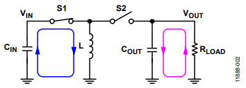
Figure 2. Current flow path during on time.

Figure 3. Current flow path during off time.
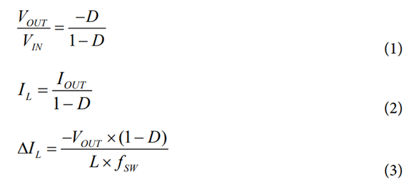
The steady state conversion ratio can be written per Equation 1 by applying the principles of inductor voltage-second balance and capacitor charge balance on the topology. The dc inductor current value, IL, in CCM is specified in Equation 2, and the inductor ripple current, ∆IL, is shown in Equation 3.
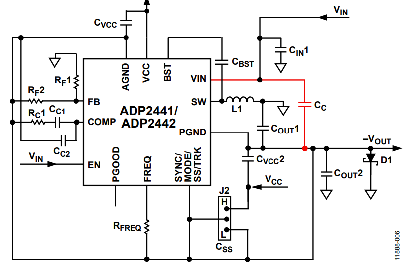
Implementation with the ADP2441/ADP2442
To implement the buck boost topology inverting power supply application by using the ADP2441/ADP2442 synchronous buck regulator, take into consideration some design restrictions as listed in Table 1.
| Voltage and Current | Device Parameters | ADP2441/ADP2442 | |
| VIN_MIN | > | VUVLO | 4.5 V |
| VIN_MIN + |VOUT| | < | VMAX | 20 V |
| IL_PEAK (IL_peak not = IOUT) | < | IOCP | 1.2 A/1.2 A |
The minimum input voltage of the buck boost circuit must be higher than the UVLO voltage of the ADP2441/ADP2442, which has the typical value of 4.5 V to get the regulator to work. The sum of the maximum input voltage and the absolute value of the output voltage must be lower than the maximum operation input voltage of the regulators, VMAX, which has the typical value of 20 V. In addition, make sure the inductor peak current is smaller than the OCP trigger point of the regulator with accommodation for inductance tolerance.
To convert the synchronous buck regulator into the buck boost topology, the inductor and output capacitor are connected similar to the buck topology. Note that the ground and the output voltage points are reversed as shown in Figure 4.


Output Voltage Setting
The output voltage is set by an external resistive divider. The resistor values are calculated using
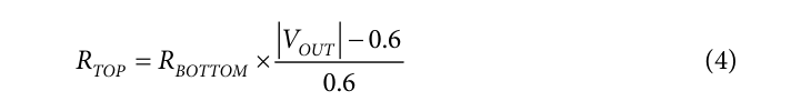
To limit the output voltage accuracy degradation due to the FB bias current (0.1 µA maximum) to less than 0.5% (maximum), ensure that RBOTTOM < 30 kΩ.
Table 2 lists the recommended resistor divider for various output voltages.
| VOUT (V) | RTOP ± 1% (kΩ) | RBOTTOM ± 1% (kΩ) |
| −1.2 | 10 | 10 |
| −1.8 | 20 | 10 |
| −2.5 | 47.5 | 15 |
| −3.3 | 10 | 2.21 |
| −5 | 22 | 3 |
| −12 | 28 | 1.47 |
| −15 | 35.7 | 1.5 |
Inductor Selection
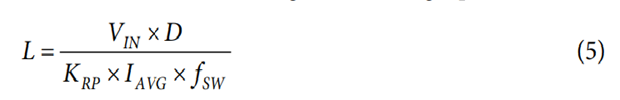
The inductor value is determined by the operating frequency, input voltage, and inductor ripple current. Using a smaller inductance leads to a faster transient response, but degrades efficiency due to a larger inductor ripple current. Using a larger inductance value leads to a smaller ripple current and better efficiency, but results in a slower transient response.
As a guideline, the inductor ripple current (∆IL) is typically set to 30% of the maximum inductor average current, IAVG. The inductor value is calculated using the following equation:
where:
VIN is the input voltage.
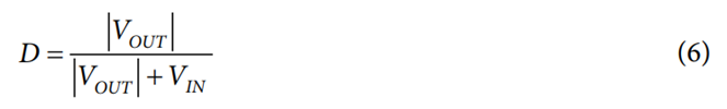
D is the duty cycle:
KRP is the chosen current ripple percentage. A good rule of thumb is around 30%.
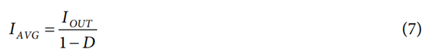
IAVG is the average inductor current:
fSW is the switching frequency.
Ramp Compensation
As with all current mode converters, the ADP2441/ADP2442 in an inverting buck boost topology require ramp compensation to assure current mode stability. The ADP2441/ADP2442 use an innovative adaptive ramp scheme that is dependent on duty cycle. This results in an ideal ramp compensation amplitude over a wider range of duty cycle than could be achieved with the old style fixed ramp compensation that many chips use. To choose an inductor that will be current-mode stable first, choose an inductor using Equation 5. Then check that Qn calculated using Equation 8 is between 0.2 and 0.9 at both minimum and maximum VIN. Equation 8 is based on Ridley’s work in his An Accurate and Practical Small-Signal Model for Current-Mode Control paper (see the References section).

where:
fSW is the switching frequency.
The peak inductor current is calculated by adding the dc component and half of the peak-to-peak inductor ripple current.
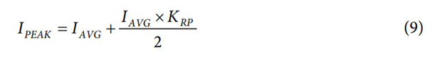
The peak inductor current is also the peak current in the internal power switch, which is the sense element used to determine whether to induce current limit. To avoid premature current limit, the peak inductor current should not exceed the OCP threshold current, IOCP, of the devices.
Taking into account this maximum peak inductor current, the application space of the ADP2441/ADP2442 in the inverting buck boost topology for common input voltages at 600 kHz switching frequency is shown in Figure 5 with the assumption that the peak-to-peak inductor ripple current is 40% of the inductor average current.


The saturation current of the inductor must be larger than the peak inductor current. For ferrite core inductors with a steep saturation characteristic, the saturation current rating of the inductor should be higher than the current limit threshold for the IC. This prevents the inductor from saturating during normal operation.
Output Capacitor Selection
The output voltage of the inverting buck boost tends to be noisier than a buck converter. This is because unlike a buck converter, the output current is discontinuous in the inverting buck boost topology. The fast rise and fall times of Switch S2 result in noise spikes on the output voltage as the current in S2 is ramped up quickly from 0 to IL and back to 0. This makes it very important to use low ESR, MLCC capacitors and good layout techniques to reduce parasitic inductance.
Equation 10 gives an estimated value of the minimum capacitance required to keep the output voltage ripple within an allowable range.
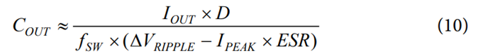
where:
∆VRIPPLE is the allowable output ripple voltage. ESR is the total equivalent series resistance of the output capacitors.
IPEAK is the inductor peak current.
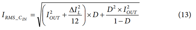
To achieve as low output ripple voltage as possible, MLCC capacitors that have very low ESR values are recommended. The rms current rating of the selected output capacitors should be larger than the values calculated using Equation 11.

Input Capacitor Selection
The input current is also discontinuous in the inverting buck boost topology. Therefore, the fast rise and fall times of Switch S1 result in noise spikes on the input rail as the current in S1 is ramped up quickly from 0 to IL and back to 0. This makes it very important to use low ESR, MLCC capacitors, and good layout techniques to reduce parasitic inductance.
Equation 12 calculates the minimum input capacitance assuming energy depletion of the input capacitor during on time is no more than 5% of the input voltage.
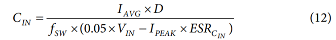
where:
IAVG is the average inductor current.
ESRCIN is the equivalent series resistance of the input capacitors.
At least one 10 µF ceramic capacitor is recommended; place it as close to PVIN pin as possible. The rms current of the selected input capacitor should be greater than the value calculated in Equation 13.
Although the majority of the capacitance on the input voltage rail is referenced to system ground, an additional input decoupling capacitor placed from the input voltage to the GND pin of ADP2441/ADP2442 can reduce the output voltage ripple and improve the transient response as shown in Figure 6.

Compensation Selection
The control-to-output transfer function of the power stage in buck boost topology can be written in the form:
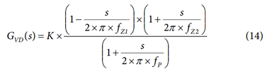
where:
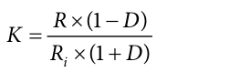
R is the load resistor.
Ri is the current sense gain with a typical value of 0.49 V/A.
The transfer function GVD(s) has one right-half-plane-zero (RHPZ), fZ1; one zero, fZ2; and one pole, fP. The values of the zero and pole are:
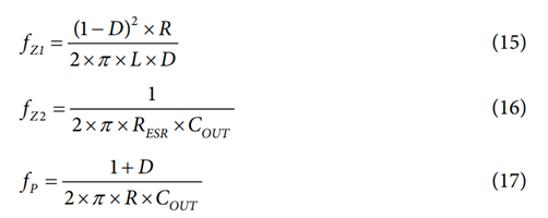
where:
RESR is the equivalent series resistance of the output capacitor.
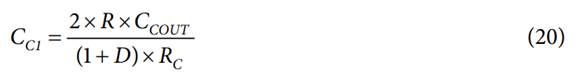
Use the following design guidelines to calculate the values of the compensation network components
- Set the cross frequency, fC, between fP and 1/3 of fZ1:

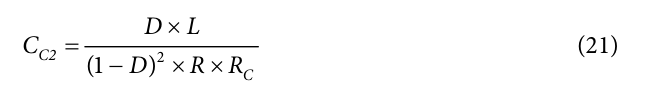
- Calculate the RC value using the equation:
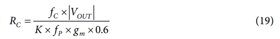
where:
gm is the transconductance of the internal error amplifier with a typical value of 250 µS.
- Place the compensation zero at 1/2 of the power stage pole, fP:
- Place the compensation pole at the RHPZ fZ1:
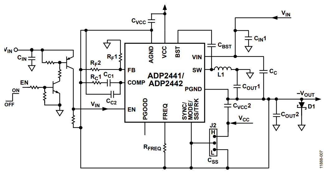
Enable Signal Level Shifting
The ADP2441/ADP2442 have an EN pin to enable and disable the regulator. However, in the inverting buck boost application, the IC is referenced to the negative output voltage instead of the system ground. Once the chip is enabled, pulling the enable pin to ground will not turn the IC off because the voltage from the enable pin to AGND of the IC will be equal to VOUT.
One of the possible solutions for this issue is to use NPN and PNP transistors and several resistors to level shift the enable level as shown in Figure 7.
Note that the precision enable feature of the ADP2441/ADP2442 is lost when the level shifting circuit is used. If the enable function is not needed, simply connect the EN pin to the input voltage as shown in Figure 4.

VOUT Over Shoot before Startup
When using the synchronous buck regulator as an inverting buck boost topology, one common issue is that the output voltage starts off positive before the regulator is enabled as shown in Figure 8.

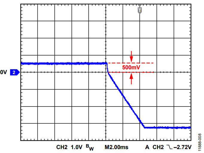
This positive output voltage is caused by the shutdown current of the regulator and any other chips connected to the negative rail, flowing from the PGND pin of the IC through the body diode of the low-side MOSFET and back to the system ground as shown in Figure 9. The body diode of the low-side MOSFET is that which clamps the VOUT at the forward voltage of the body diode with a typical value of around 500 mV.


Because VOUT is connected to the PGND pin of the regulator which is actually the reference point for the internal circuits like UVLO, the positive voltage shown in the PGND pin decreases the UVLO threshold voltage. The regulator may fail to start up when the input voltage is very close to the UVLO threshold voltage of the regulator, which has a typical value of 4.0 V
This issue can be seen in all buck regulators when they are used to perform the inverting buck boost topology described herein and it is very hard to eliminate the issue completely. One solution is to put a Schottky diode on the output of the converter. This diode reduces the positive voltage somewhat and prevents any silicon diodes in the ADP2441/ADP2442 regulator or any load components from turning on and causing problems. Another solution is to reduce the resistance of the feedback resistor divider until the voltage drop across the resistor divider is lower than the forward voltage of the body diode of the low-side MOSFET. Then, the shutdown current flows through the resistor divider instead of the body diode as shown in Figure 10 and the positive voltage on the PGND pin can be reduced to an acceptable value.

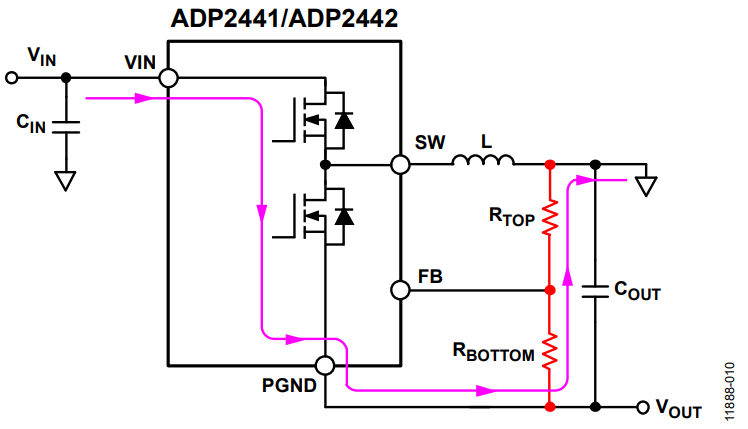
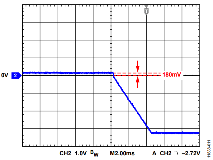
Figure 11 shows the result of reducing the resistance of the resistor divider. The positive VOUT voltage decreases from 500 mV to 180 mV.

The drawback of this solution is that the quiescent current of the system increases because the current flowing through the feedback resistor is higher. This increased quiescent current can reduce the efficiency at light loads quite a bit, though the actual power loss is quite small.
Conclusion
The ADP2441/ADP2442 can be used successfully in the inverting buck boost topology resulting in a simple, inexpensive, and small solution for creating a negative rail. In addition to detailing all of the necessary design equations, this application note provides a simple EN level shifting circuit when the enable/disable functionality is needed. Also, the potential start-up issue inherent with the inverting buck boost topology is avoided with two simple solutions.
By following the design equations and suggestions in this application note, the system designer can ensure a robust design that satisfies all their requirements.
References
R. B. Ridley. An Accurate and Practical Small-Signal Model for Current-Mode Control. Ridley Engineering Inc. 1999.
Authors

