Objective
The objective of this lab activity is to build the various CMOS logic functions possible with the CD4007 transistor array. The CD4007 contains three complementary pairs of NMOS and PMOS transistors.
Making Inverters with the CD4007 Transistor Array
Figure 1 shows the schematic and pinout for the CD4007.


As many as three individual inverters can be built from one CD4007 package. The first, and simplest to configure, as shown in Figure 2, is built by connecting pins 8 and 13 together as the inverter output. Pin 6 will be the input. Be sure to connect Pin 14 (VDD) to the power supply and Pin 7 (VSS) to the ground.


The second inverter is made by connecting Pin 2 to VDD and Pin 4 to VSS. Pins 1 and 5 are connected together as the output and with Pin 3 as the input. The third inverter is made by connecting Pin 11 to VDD and Pin 9 to VSS. Pin 12 is the output and Pin 10 is the input.
Characterizing the CMOS Inverter
There are a number of both static (DC) and dynamic (AC) performance characteristics of the CMOS inverter that are often specified and should be measured. In this section, we will measure a number of them for the inverter, but these same measurements can be made on other types of gates we will see in later sections of this activity. We will start with the static characteristics: threshold voltage, transition region width, output source, and sink current.
Threshold Voltage
Generally, the CMOS fabrication process is designed such that the threshold voltage, VTH, of the NMOS and PMOS devices are roughly equal; that is, complementary. The designer of the inverter then adjusts the width to length ratio, W/L, of the NMOS and PMOS devices such that their respective transconductance is also equal.
Directions
On your solderless breadboard, build the first inverter shown in Figure 2 to test the input to output switching characteristics of the CMOS inverter. The blue boxes in Figure 3 indicate the required connections to the connector on the ADALM2000. Connect VP (5 V) power to VDD (Pin 14) through a 100 Ω resistor to measure the supply current and ground to VSS (Pin 7). Connect the output of the waveform generator to the inverter input (Pin 6) along with Scope Input 1+ and connect the inverter output (pins 8 and 13) to Scope Input 2+. It is also generally good to ground the unused negative scope inputs (1–, 2–).


Hardware Setup
Configure the waveform generator for a 100 Hz triangle wave with 5 V amplitude peak-to-peak and 2.5 V offset. Both scope channels should be set to 1 V/ div. Configure the scope in XY mode with Channel 1 on the horizontal axis and Channel 2 on the vertical axis.


Procedure
First, using the Scope Channel 2 to measure the inverter output voltage vs. the input as the input is swept from 0 V to 5 V, obtain a plot like the top curve in Figure 5.
Next, move the Channel 2 Scope Inputs 2+ and 2– to measure the voltage across the 100 Ω resistor, R1, in Figure 3. You may need to adjust the vertical scale of Channel 2 for an optimal view of the current waveform. Now obtain a plot of ID vs. the input as the input is swept from 0 V to 5 V. This should give you a plot much like the bottom curve in Figure 5.


The input to output transfer characteristic plots the output voltage VOUT vs. the input voltage VIN. Notice that when the input voltage increases from 0 V to 5 V, the output voltage decreases from 5 V to 0 V. The supply current characteristic plots the current flowing through the transistors between VDD and the ground also vs. the input voltage VIN. The fact that there are two parts of the characteristic curves when the input voltage is near the ground and VDD, and that no current flows between VDD and the ground is attractive because there is no power dissipation at this stage. This very fact is the reason that nearly all digital circuitry today is now built using CMOS technology.
The width of the transition region as a fraction of the power supply leads to a performance measure that is often referred to as the noise margin, the part of the input range where the output remains at a constant high or low level. Given that there is likely to be noise superimposed on the input signal, it is desirable to have the output not respond to small changes in the input. A narrow transition region also potentially reduces the amount of time the output spends transitioning between states and, thus, reduces the shoot-through current when both the NMOS and PMOS transistors are partially turned on.
Dynamic Performance
In this section, we will investigate the dynamic properties of the CMOS inverter; that is, its behavior when switching the input signal from low to high or high to low voltages, and the associated power dissipation.
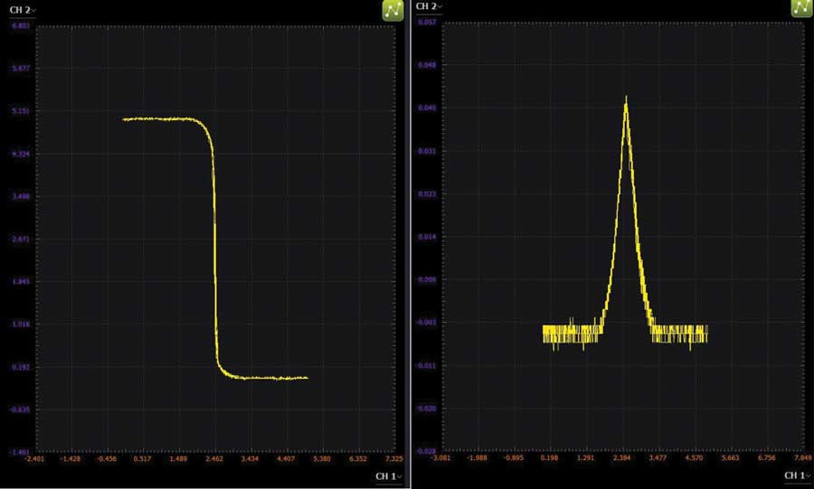
We now consider a CMOS inverter driven by a voltage pulse. Typical input/output waveforms are shown in Figure 5. Delay characterization of the dynamic behavior of an inverter is given by two propagation delay times, THL and TLH, as illustrated in Figure 7. Note that these propagation times are specified with respect to the mid supply voltage VDD/2.


Hardware Setup
Now configure the waveform generator for a 500 kHz square wave with a 5 V amplitude peak-to-peak and 2.5 V offset. Be sure to reconnect the Scope Channel 2 to measure the output voltage waveform. Both scope channels should be set to 1 V/div. Adjust the horizontal scale so that you can view both the rising and falling edges of the input and output waveforms similar to what is shown in figures 7 and 8.


Procedure
Configure the oscilloscope Channel 1 and Channel 2 to capture several periods of the input and the output signals. A Scopy plot example is presented in Figure 10.


Measurements
Propagation delay, THL and TLH = time, between input transition (when VIN = VDD/2) and output transition (when VOUT = VDD/2). Rise time, TR = time for a waveform to rise from 10% to 90% of its steady state value. Fall time, TF = time for a waveform to fall from 90% to 10% of its steady state value.
Making a CMOS Schmitt Trigger with the CD4007 Transistor Array
Directions
The input of the Schmitt trigger, as shown in Figure 11, is tied to the gates of four stacked devices. The upper two are PMOS and the lower two are NMOS. Transistors M5 and M6 operate as source followers and introduce hysteresis by feeding back the output voltage, VOUT, to the two points in the stack midway between the two NMOS and two PMOS devices.


When VIN is at 0 V, transistors M1 and M3 are on, and M2, M4, and M5 are off. Since VOUT is high, M6 is on and acts as a source follower, and the drain of M2, which is also the source of M4, is at VDD to VTH. If the input voltage is ramped up to one threshold above the ground transistor, M2 begins to turn on, and M2 and M6, both being on, form a voltage divider network biasing the source of M4 at roughly half the supply. When the input is a threshold above 1/2 VDD, M4 begins to turn on and regenerative switching is about to take over. Any more voltage on the input causes VOUT to drop. When VOUT drops, the source of M6 follows its gate, which is VOUT. The influence of M6 in the voltage divider with M2 rapidly diminishes, bringing VOUT down further yet. Meanwhile M5 has started to turn on, its gate being brought low by the rapidly dropping VOUT. M5 turning on brings the source of M3 low and turns M3 off. With M3 off, VOUT will collapse all the way down to ground. The snapping action is due to greater than unity loop gain through the stack caused by a positive feedback through the source follower transistors. When the input is brought low again, a similar process occurs in the upper portion of the stack, and the snapping action takes place when the lower threshold its reached.
Hardware Setup
On your solderless breadboard, build the Schmitt trigger circuit shown in Figure 11 to test the input to output switching characteristics as you did with the plain inverter.
Configure the waveform generator for a 1 kHz triangle wave with a 5 V amplitude peak-to-peak and 2.5 V offset. Both scope channels should be set to 1 V/div. Configure the scope in XY mode with Channel 1 on the horizontal axis and Channel 2 on the vertical axis.


Procedure
Use Scope Channel 2 to measure the output voltage vs. the input, as the input is swept from 0 V to 5 V. Obtain a plot like you did for the simple inverter.


Making a NAND/AND Gate with the CD4007 Transistor Array
As shown in Figure 14, one 2-input NAND gate and one inverter can be built from one CD4007 package. Configure the NAND gate as shown in Figure 14 by connecting pins 12 and 13 together as the NAND output. Pin 14 and Pin 11 are connected to VDD for power and Pin 7 (VSS) to the ground. Pin 9 should be tied to Pin 8 to complete the N side of the NAND gate. Pin 6 will be the A input and Pin 10 will be the B input.


The inverter is made by connecting Pin 2 to VDD and Pin 4 to VSS. Pins 1 and 5 are connected together as the output and with Pin 3 as the input. An AND gate is made by connecting the output of the NAND at pins 12 and 13 to the inverter input at Pin 3.
A single 3-input NAND gate can be made by using all six devices as shown in Figure 17.
Directions
Build both the 2-input and 3-input NAND gates and confirm their logic function by filling out a truth table for each. You can also measure the input threshold voltage for each input as you did for the simple inverter by connecting the unused input(s) to VDD.


Question
Can you name and describe other types of logic functions that can be built with the CD4007 array?
You can find the answer at the StudentZone blog.

