Objective
By combining the circuit blocks already explored in previous StudentZone articles, this activity helps build a complete high open-loop gain amplifier from a few discrete devices.
Materials
- ADALM2000 Active Learning Module
- Solderless breadboard
- Jumper wires
- One 8.2 kΩ resistor (a close approximation can be made by connecting your 1.5 kΩ and 6.8 kΩ in series)
- One 47 kΩ resistor
- One 100 kΩ resistor
- Two 470 kΩ resistors
- One 10 kΩ resistor
- One 1 kΩ resistor
- Two 22 μF capacitors
- One 1 μF capacitor
- One 47 nF capacitor
- One small signal PNP transistor (2N3906)
- Three small signal NPN transistors (2N3904, SSM2212)
Description
On your solderless breadboard, construct the amplifier circuit shown in Figure 1.


Hardware Setup
Connect your circuit to the ADALM2000 I/O connector as indicated by the blue boxes in Figure 1. It is best to ground the unused negative scope inputs when not being used. The SSM2212 NPN matched pair should be used for Q1 and Q2 transistors.
Procedure
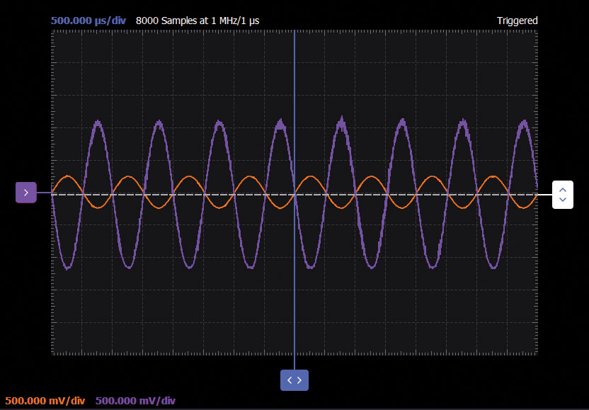
Configure a waveform generator for a 1 kHz sine wave with an amplitude of 400 mV peak-to-peak and zero offset. Using Scope Channel 1 to observe the input at W1 and Scope Channel 2 to observe the output of the amplifier at RL, record the input to output amplitude and phase relationship.
Configure the oscilloscope to capture several periods of the input and output signal, scaling the channels at a 500 mV/division.
An oscilloscope plot example is presented in Figure 3.


Unity-Gain Amplifier Objective
By combining some of the circuit blocks explored in previous articles, we can build a complete unity-gain buffer amplifier. The addition of the current mirror load for the differential stage is a key improvement to this simple amplifier.
Materials
- ADALM2000 Active Learning Module
- Solderless breadboard
- Jumper wires
- One 15 kΩ resistor (a 10 kΩ in series with a 4.7 kΩ can be substituted)
- Two small signal PNP transistors (2N3906 or an SSM2220 PNP match pair can be used)
- Six small signal NPN transistors (2N3904, use an SSM2212 NPN matched pair for Q1 and Q2; a TIP31C may be substituted for Q5 if you don’t have enough 2N3904 devices)
Directions
Construct the circuit shown in Figure 4 on your solderless breadboard. Connect your circuit to the ADALM2000 I/O connector as indicated by the blue boxes. It is best to ground the unused negative scope inputs when not being used.


Hardware Setup
The breadboard connections of the circuit are shown in Figure 5.


Procedure
Configure AWG1 for a 1 kHz sine wave with an amplitude of 2 V peak-to-peak and zero offset. Using Scope Channel 1 to observe the input at W1 and Scope Channel 2 to observe the output of the amplifier, record the input to output amplitude and phase relationship.
Configure the oscilloscope to capture several periods of the input and output signal, scaling the channels at a 1 V/division.
An oscilloscope plot example is presented in Figure 6.


Questions:
- For the circuit in Figure 1, what is the gain from the input source, W1, to the output seen at RL? Which components set this gain?
- Change the value of compensation capacitor C3. How does raising and lowering the value of C3 affect the frequency response?
You can find the answers at the StudentZone blog.
Appendix: More Advanced Versions on a PC Board
PC board design files for this experiment and other related extensions can be found on the ADI GitHub education tool repository for experiment board design files. The PCB schematic is shown in Figure 7, and a photo of the board is shown in Figure 8.


The PCB uses the standard 8-pin DIP single op amp footprint and can be inserted into a solderless breadboard.

